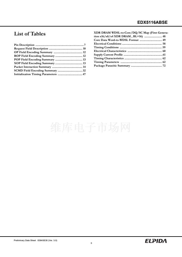
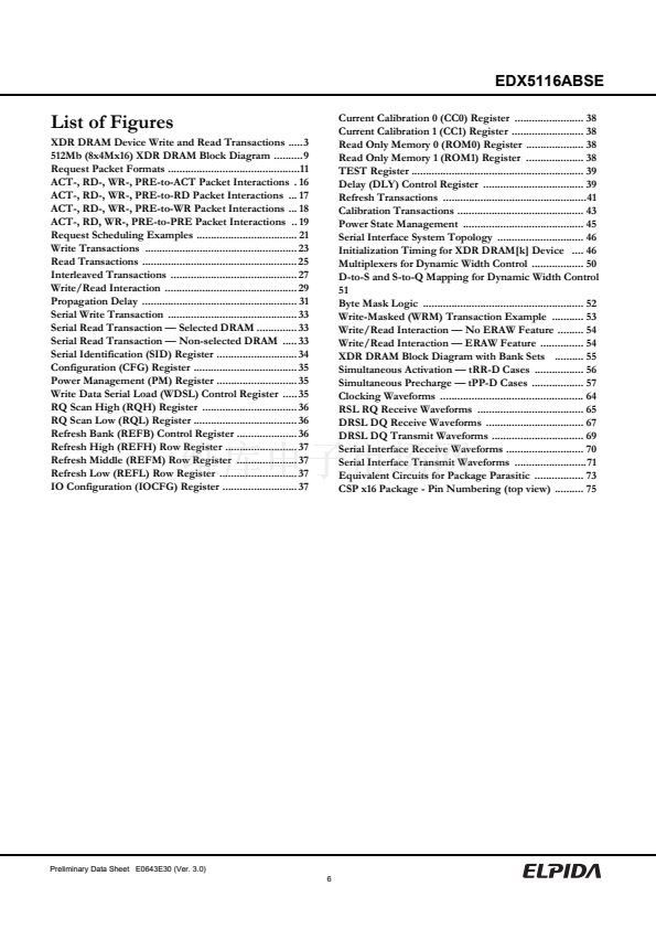
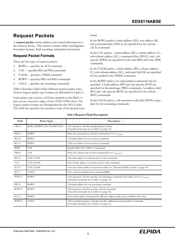
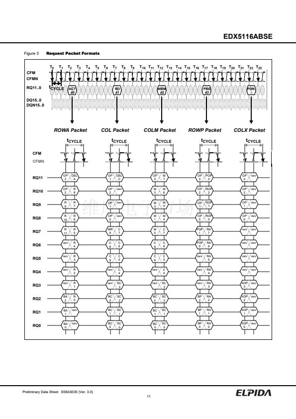
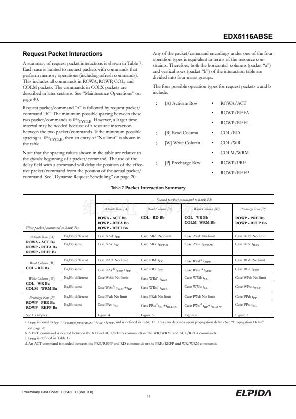
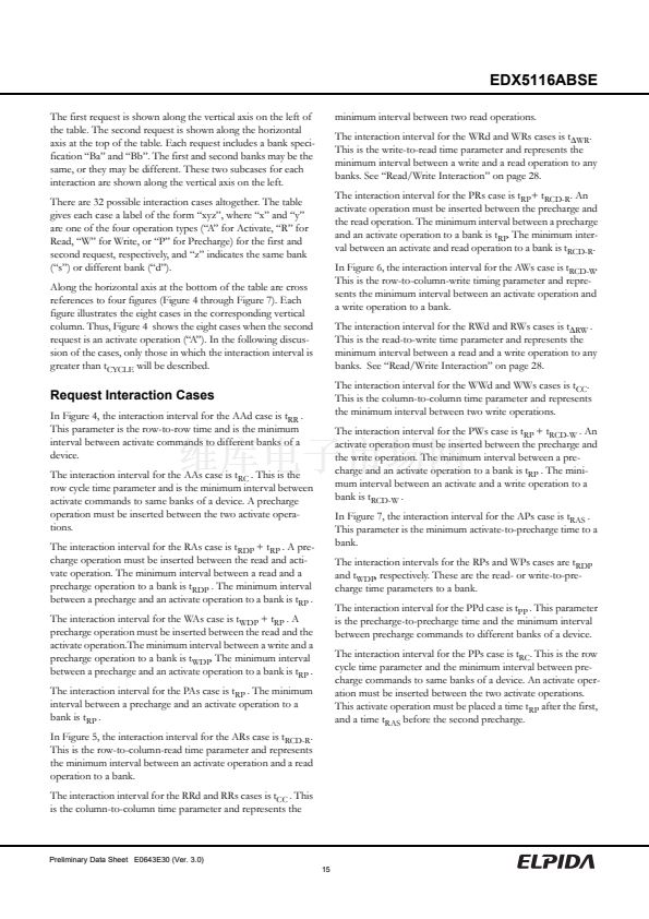
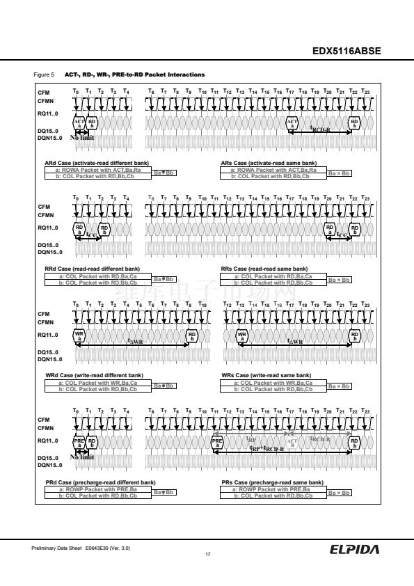
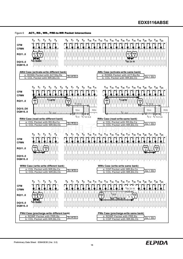
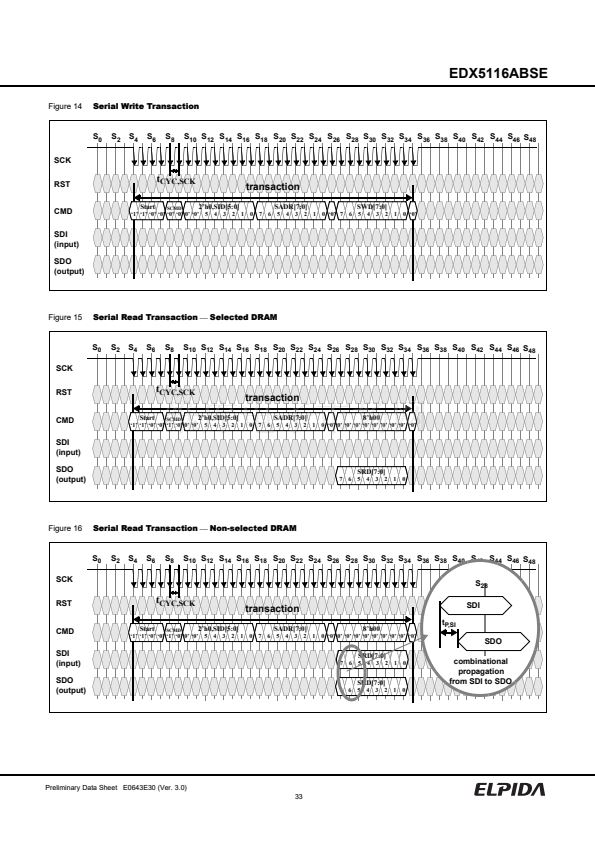
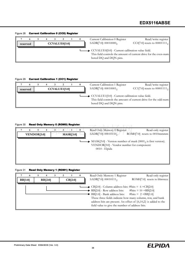
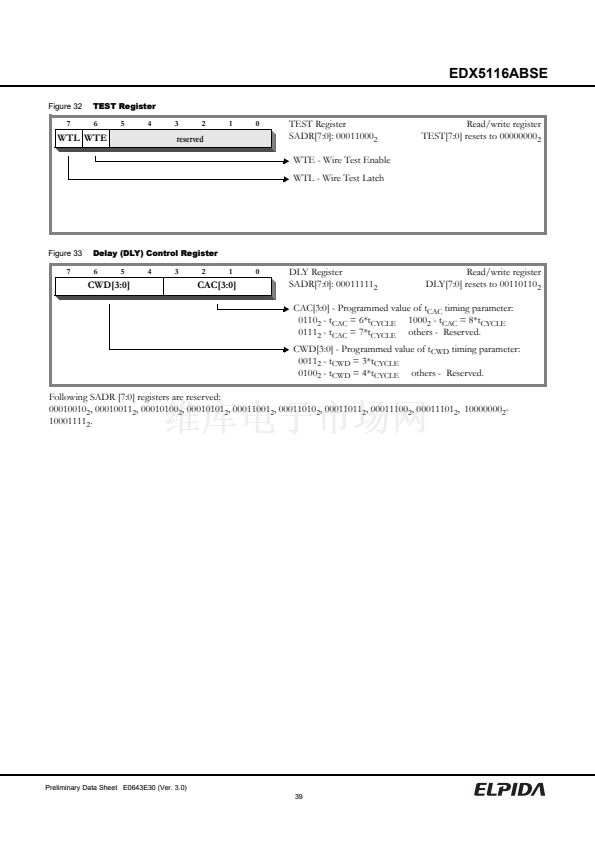
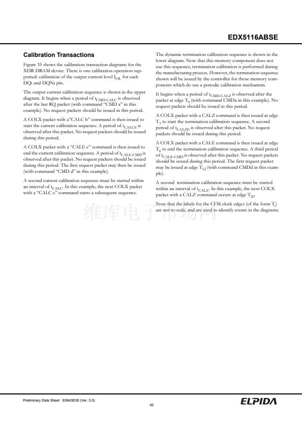
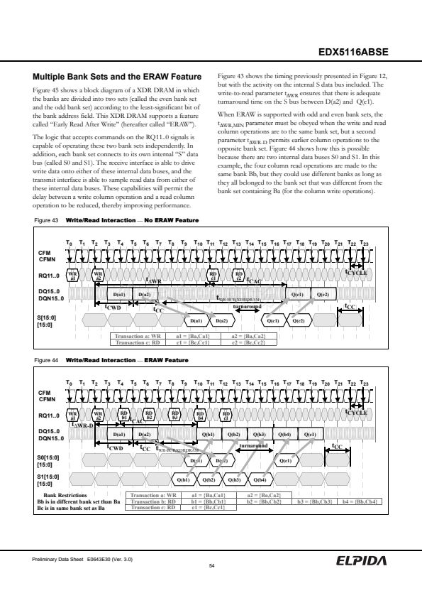
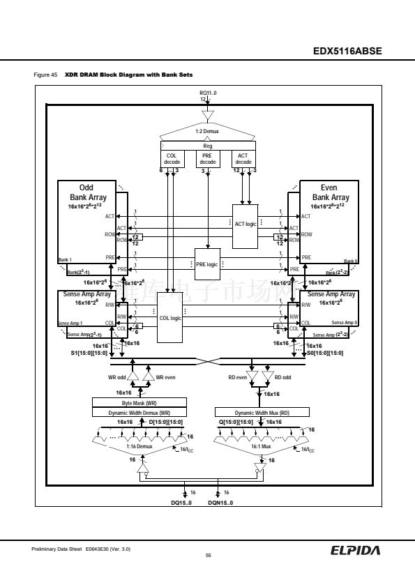
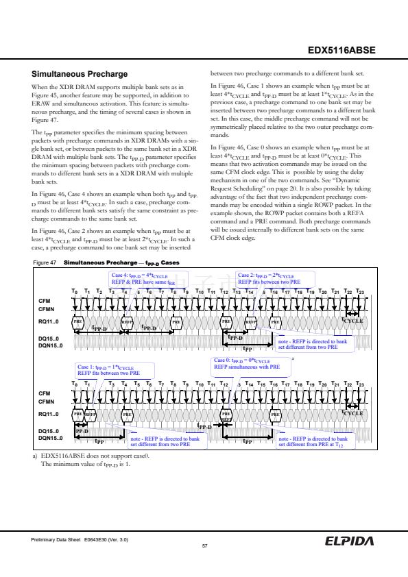
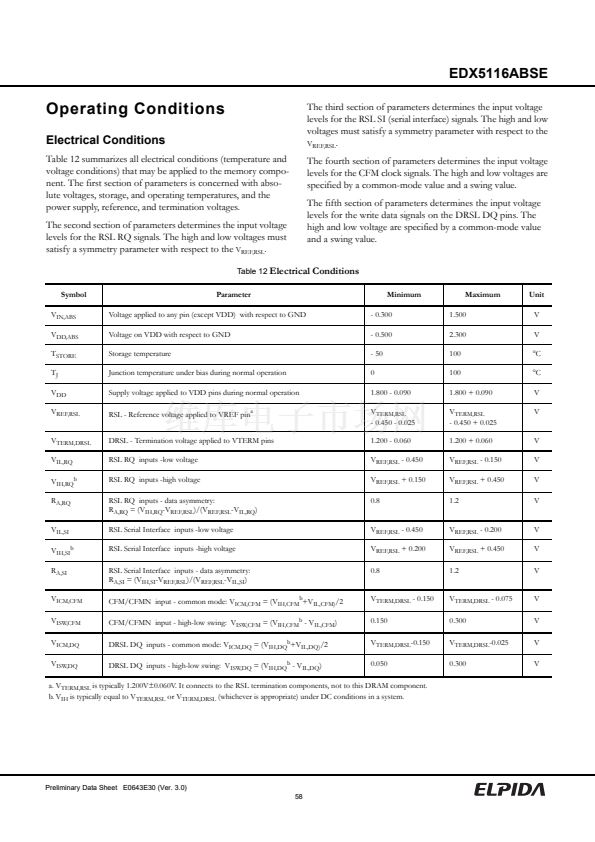
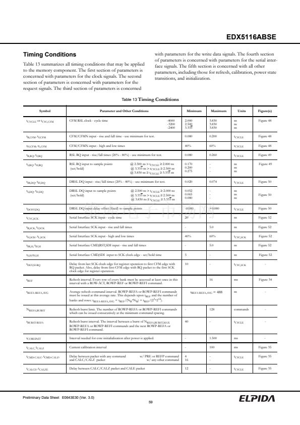
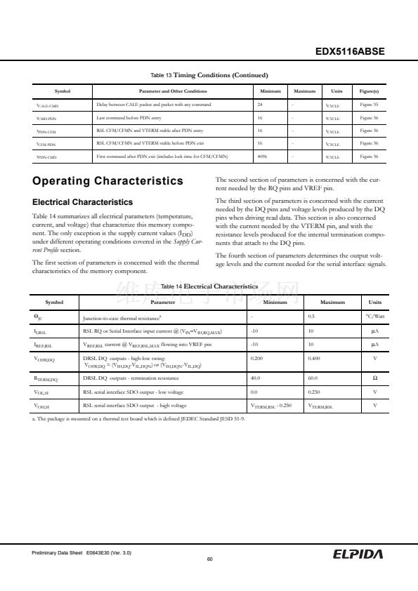
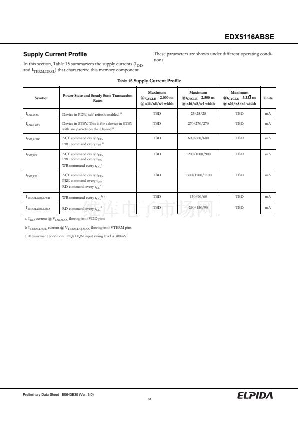
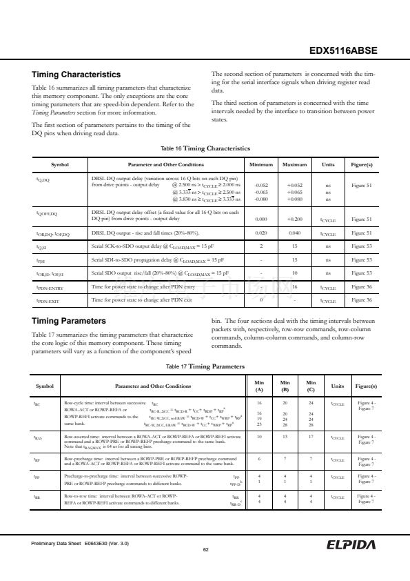
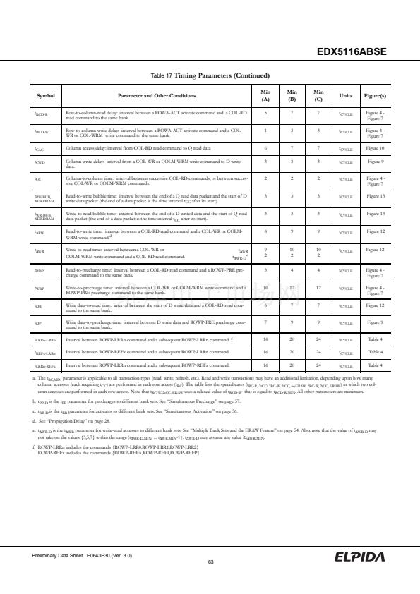
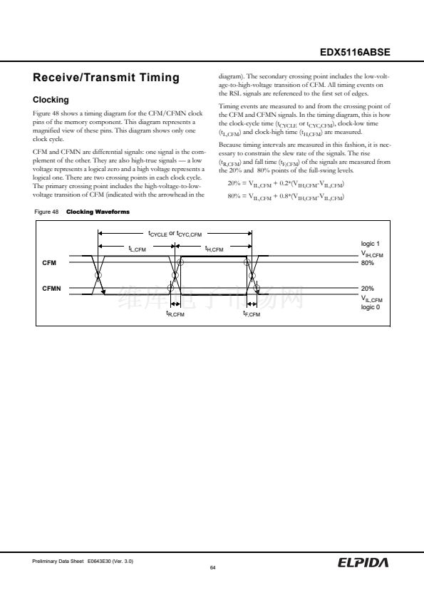
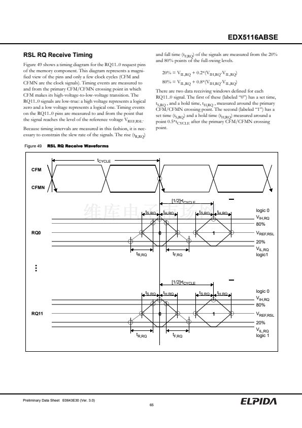
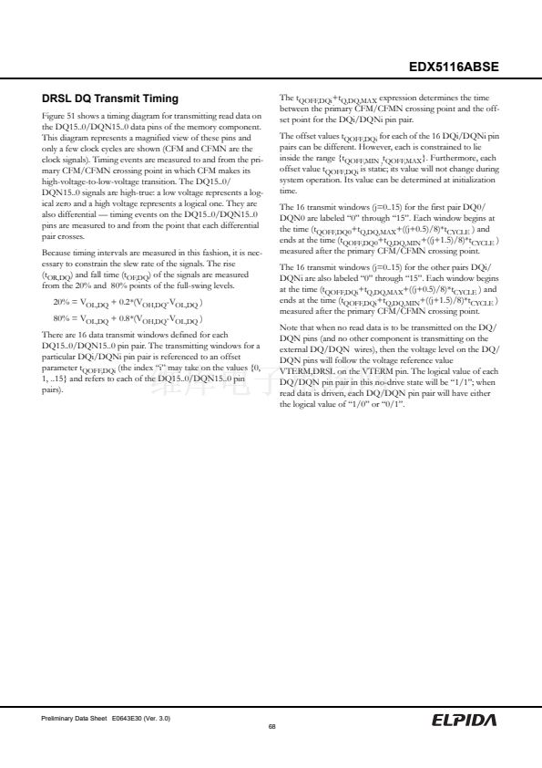
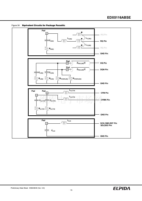
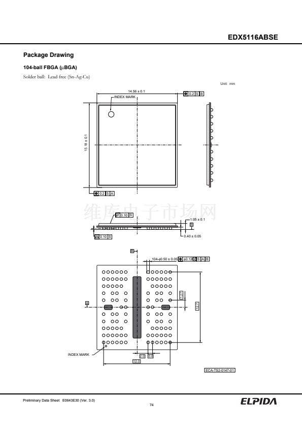
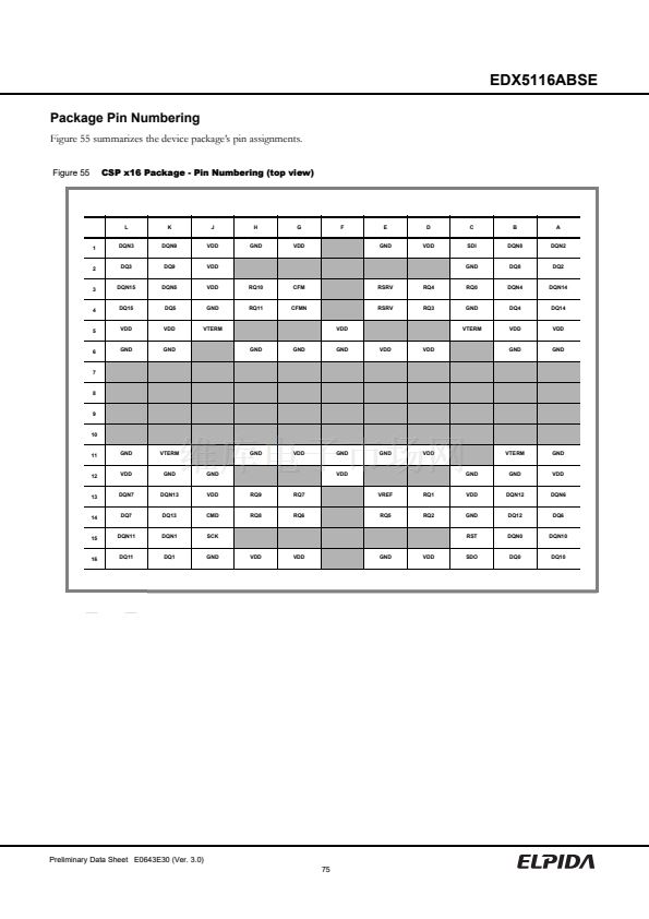
EDX5116ABSE
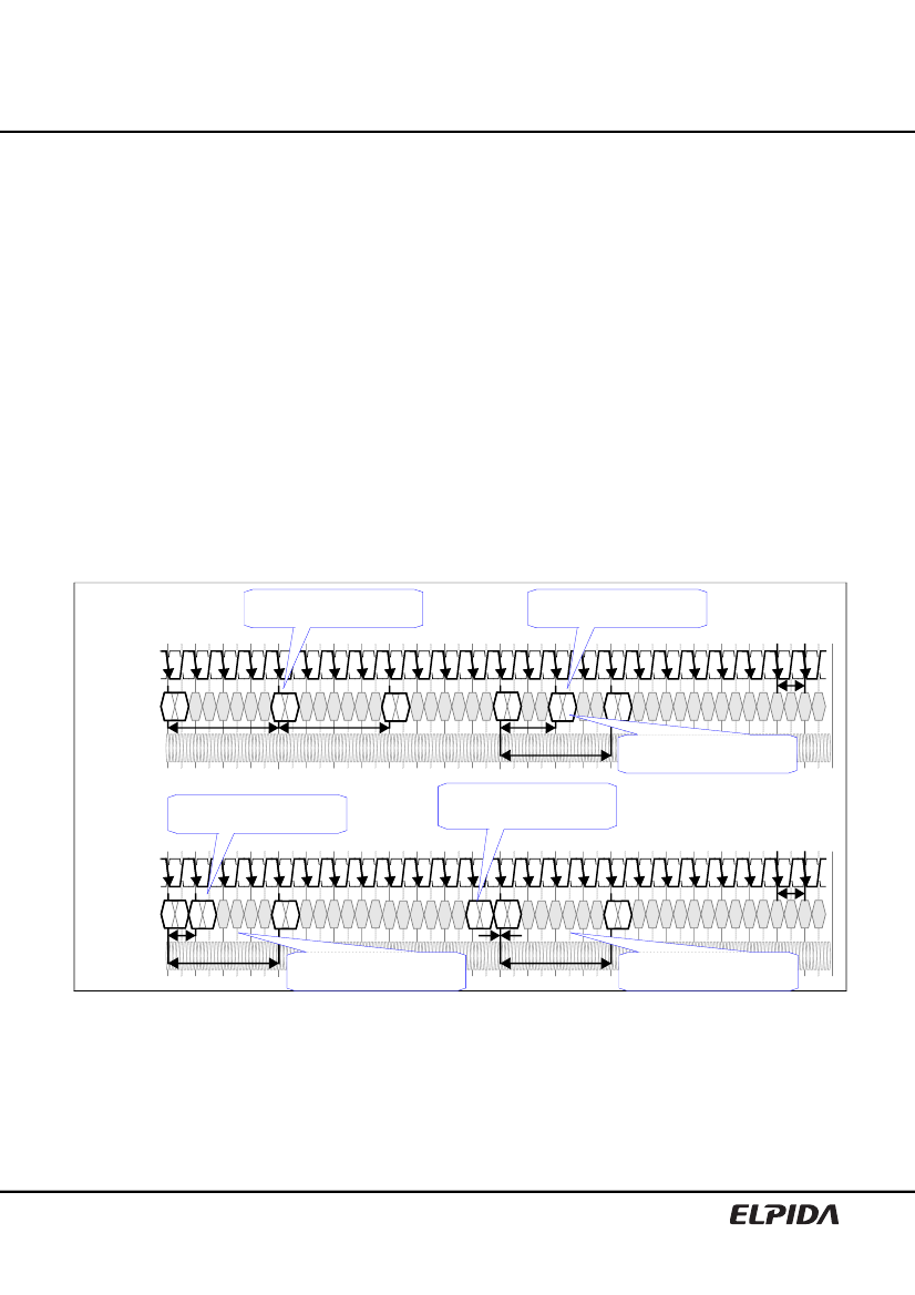
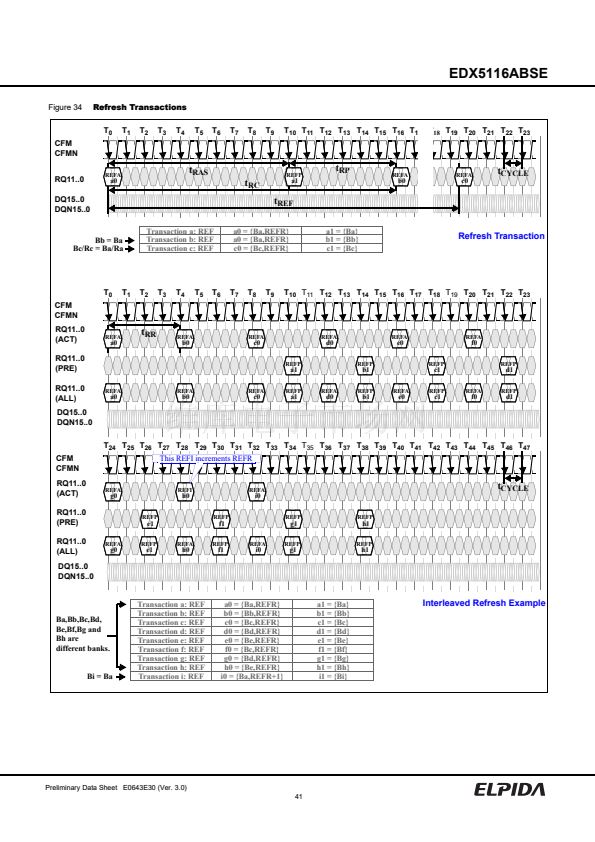
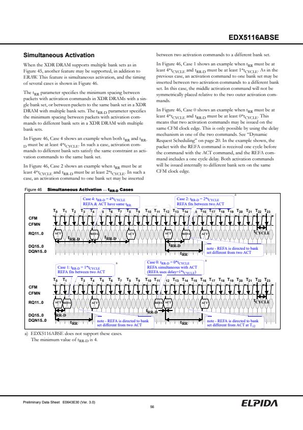
Simultaneous Activation
When the XDR DRAM supports multiple bank sets as in
Figure 45, another feature may be supported, in addition to
ERAW. This feature is simultaneous activation, and the timing
of several cases is shown in Figure 46.
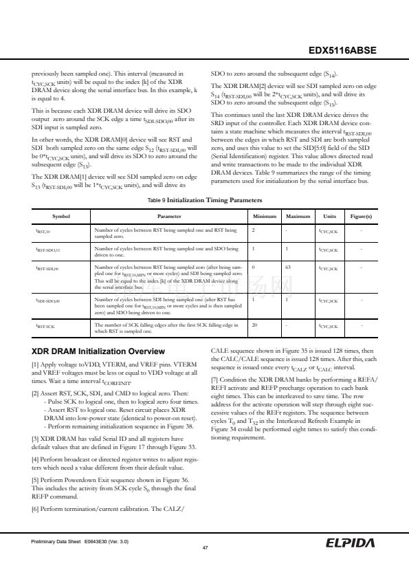
The t
RR
parameter specifies the minimum spacing between
packets with activation commands in XDR DRAMs with a sin-
gle bank set, or between packets to the same bank set in a XDR
DRAM with multiple bank sets. The t
RR-D
parameter specifies
the minimum spacing between packets with activation com-
mands to different bank sets in a XDR DRAM with multiple
bank sets.
In Figure 46, Case 4 shows an example when both t
RR
and t
RR-
D
must be at least 4*t
CYCLE
. In such a case, activation com-
mands to different bank sets satisfy the same constraint as acti-
vation commands to the same bank set.
In Figure 46, Case 2 shows an example when t
RR
must be at
least 4*t
CYCLE
and t
RR-D
must be at least 2*t
CYCLE
. In such a
case, an activation command to one bank set may be inserted
Figure 46
Simultaneous Activation
鈥?/div>
t
RR-D
Cases
Case 4: t
RR-D
= 4*t
CYCLE
REFA & ACT have same t
RR
T
0
CFM
CFMN
RQ11..0
DQ15..0
DQN15..0
a
Case 1: t
RR-D
= 1*t
CYCLE
REFA fits between two ACT
T
0
CFM
CFMN
RQ11..0
DQ15..0
DQN15..0
ACT REFA
ACT
REFA ACT
ACT
ACT
REFA
between two activation commands to a different bank set.
In Figure 46, Case 1 shows an example when t
RR
must be at
least 4*t
CYCLE
and t
RR-D
must be at least 1*t
CYCLE
. As in the
previous case, an activation command to one bank set may be
inserted between two activation commands to a different bank
set. In this case, the middle activation command will not be
symmetrically placed relative to the two outer activation com-
mands.
In Figure 46, Case 0 shows an example when t
RR
must be at
least 4*t
CYCLE
and t
RR-D
must be at least 0*t
CYCLE
. This
means that two activation commands may be issued on the
same CFM clock edge. This is only possible by using the delay
mechanism in one of the two commands. See 鈥淒ynamic
Request Scheduling鈥?on page 20. In the example shown, the
packet with the REFA command is received one cycle before
the command with the ACT command, and the REFA com-
mand includes a one cycle delay. Both activation commands
will be issued internally to different bank sets on the same
CFM clock edge.
a
Case 2: t
RR-D
= 2*t
CYCLE
REFA fits between two ACT
T
9
T
10
T
11
T
12
T
13
T
14
T
15
T
16
T
17
T
18
T
19
T
20
T
21
T
22
T
23
T
1
T
2
T
3
T
4
T
5
T
6
T
7
T
8
t
RR-D
t
RR-D
ACT
ACT
REFA
ACT
t
CYCLE
t
RR-D
t
RR
Case 0: t
RR-D
= 0*t
CYCLE
REFA simultaneous with ACT
(REFA uses delay=1*t
CYCLE
)
T
7
T
8
T
9
a
note - REFA is directed to bank
set different from two ACT
T
1
T
2
T
3
T
4
T
5
T
6
T
10
T
11
T
12
T
13
T
14
T
15
T
16
T
17
T
18
T
19
T
20
T
21
T
22
T
23
t
CYCLE
t
RR-D
t
RR
t
RR-D
note - REFA is directed to bank
set different from two ACT
t
RR
note - REFA is directed to bank
set different from ACT at T
12
a) EDX5116ABSE does not support these cases.
The minimum value of t
RR-D
is 4.
Preliminary Data Sheet E0643E30 (Ver. 3.0)
56


 1
1
 2
2
 3
3
 4
4
 5
5
 6
6
 7
7
 8
8
 9
9
 10
10
 11
11
 12
12
 13
13
 14
14
 15
15
 16
16
 17
17
 18
18
 19
19
 20
20
 21
21
 22
22
 23
23
 24
24
 25
25
 26
26
 27
27
 28
28
 29
29
 30
30
 31
31
 32
32
 33
33
 34
34
 35
35
 36
36
 37
37
 38
38
 39
39
 40
40
 41
41
 42
42
 43
43
 44
44
 45
45
 46
46
 47
47
 48
48
 49
49
 50
50
 51
51
 52
52
 53
53
 54
54
 55
55
 56
56
 57
57
 58
58
 59
59
 60
60
 61
61
 62
62
 63
63
 64
64
 65
65
 66
66
 67
67
 68
68
 69
69
 70
70
 71
71
 72
72
 73
73
 74
74
 75
75
 76
76
 77
77
 78
78
