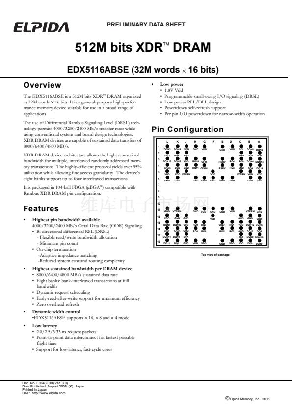
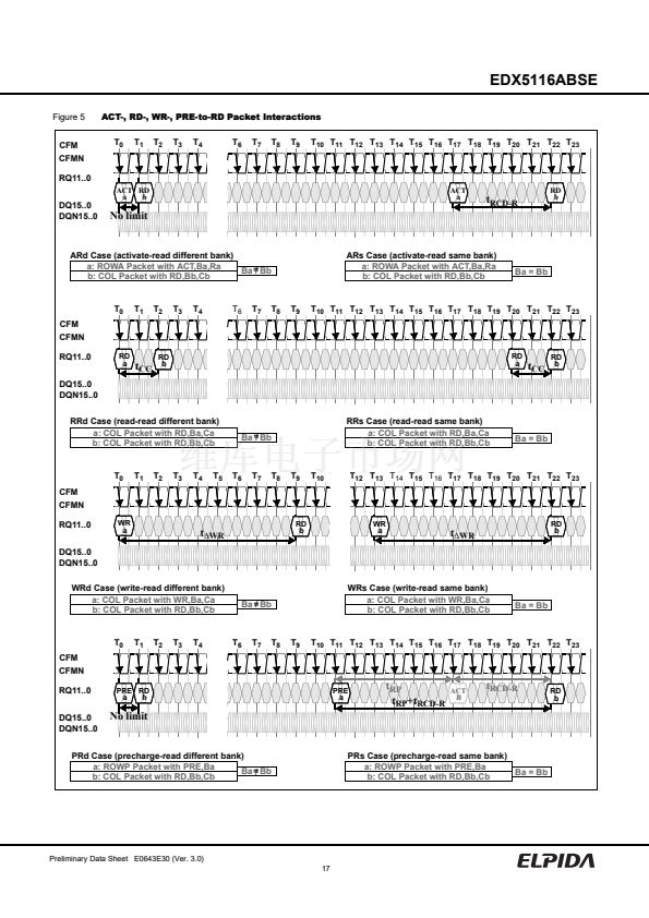
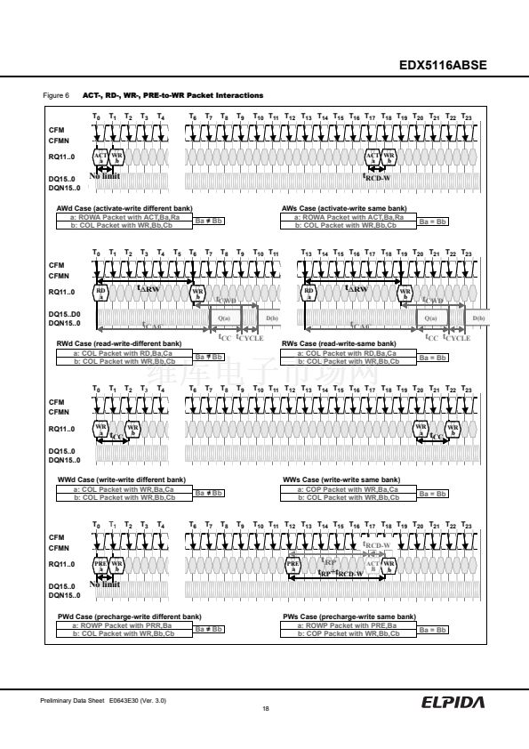
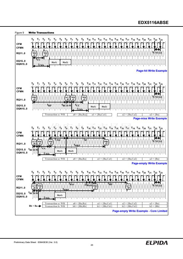
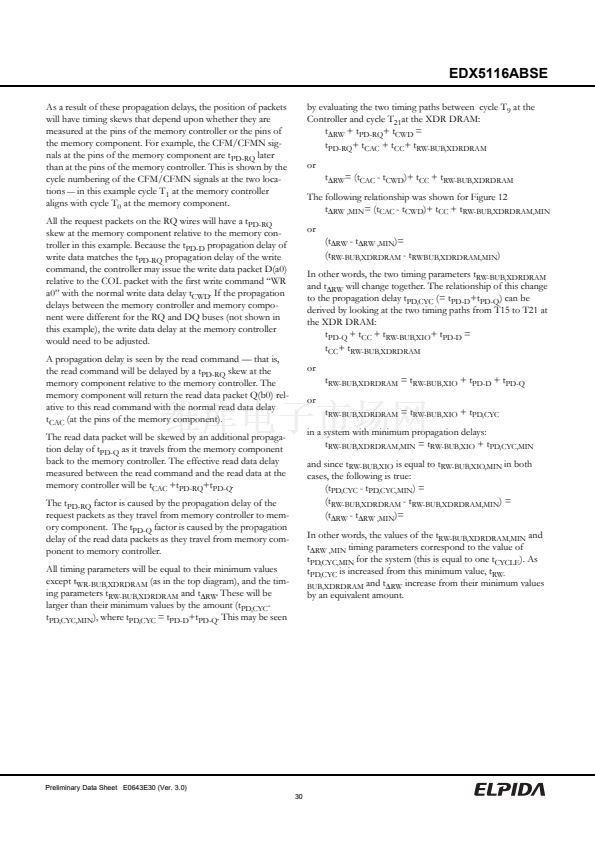
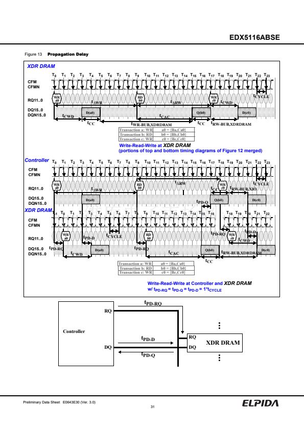
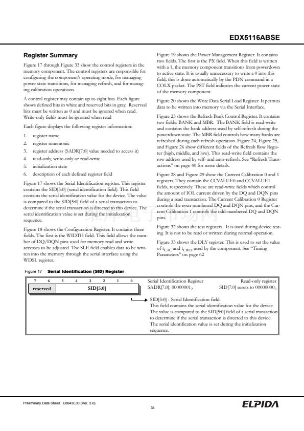
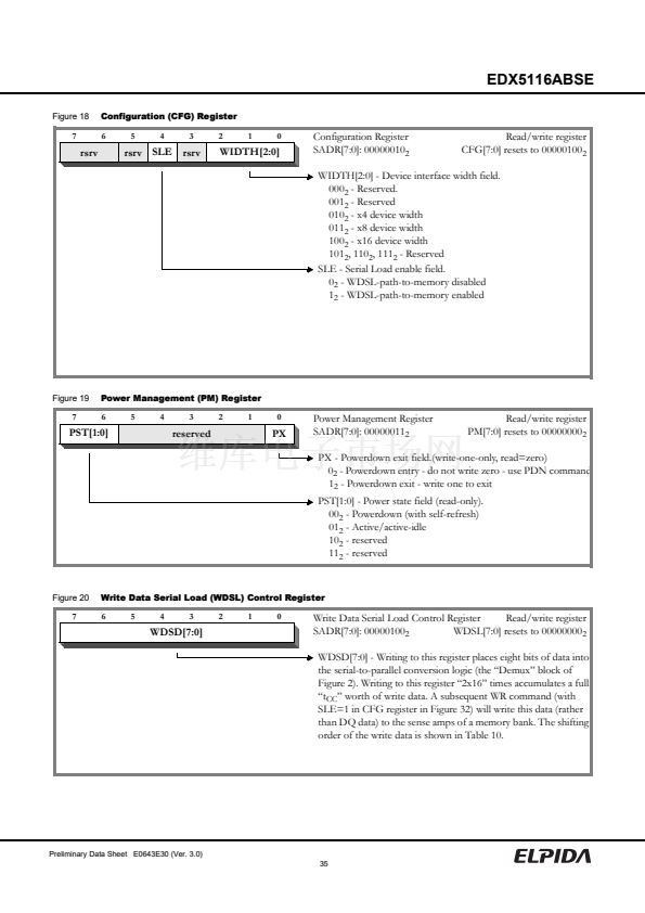
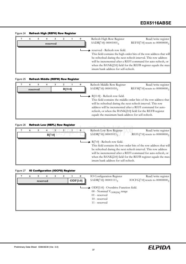
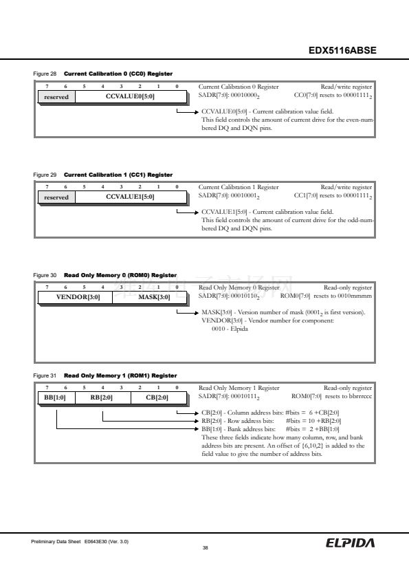
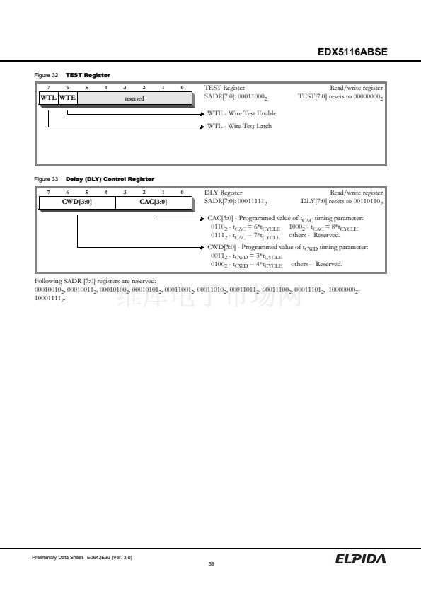
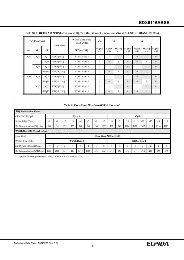
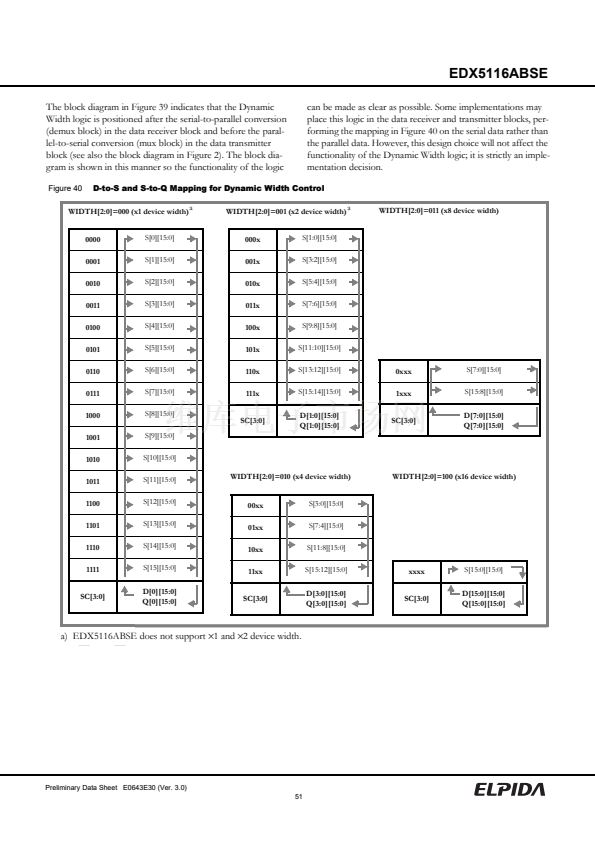
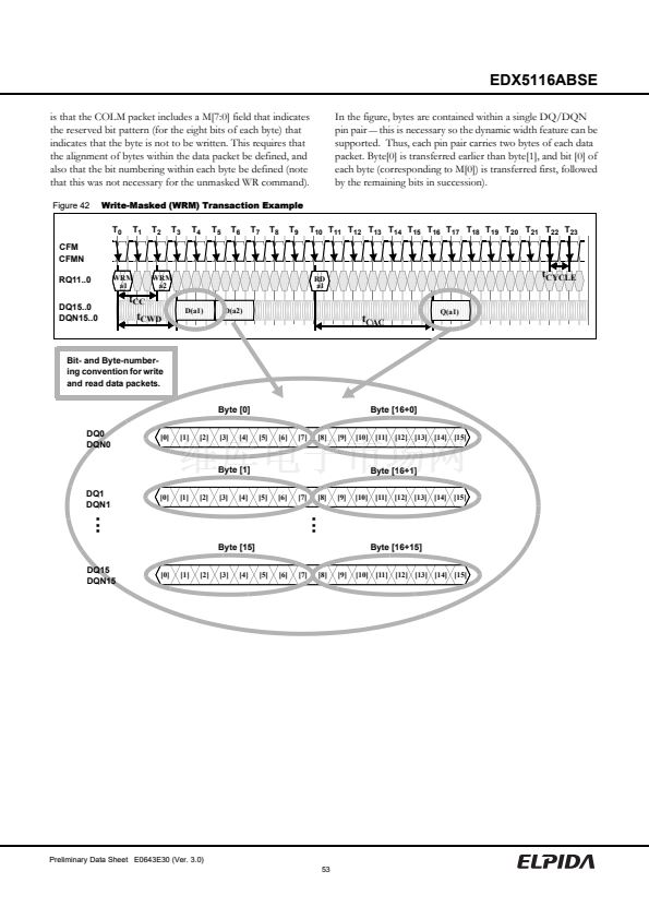
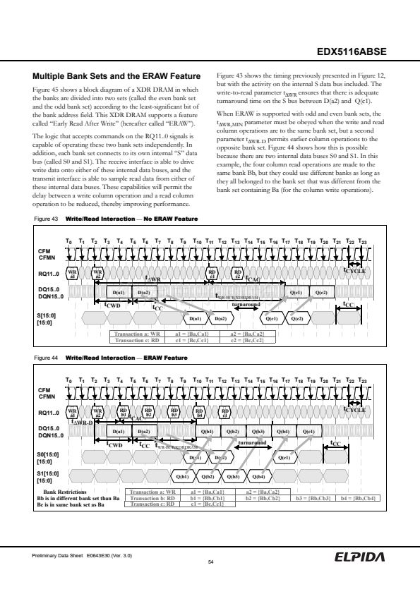
鈮?/div>
3.333 ns
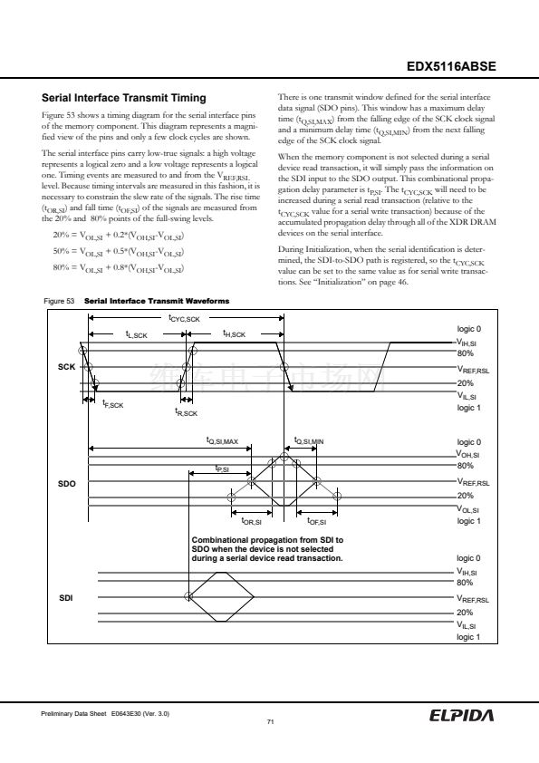
Figure 50
Figure 50
t
DOFF,DQ
t
CYC,SCK
t
R,SCK,
t
F,SCK
t
H,SCK
, t
L,SCK
t
IR,SI,
t
IF,SI
t
S,SI
,t
H,SI
t
DLY,SI-RQ
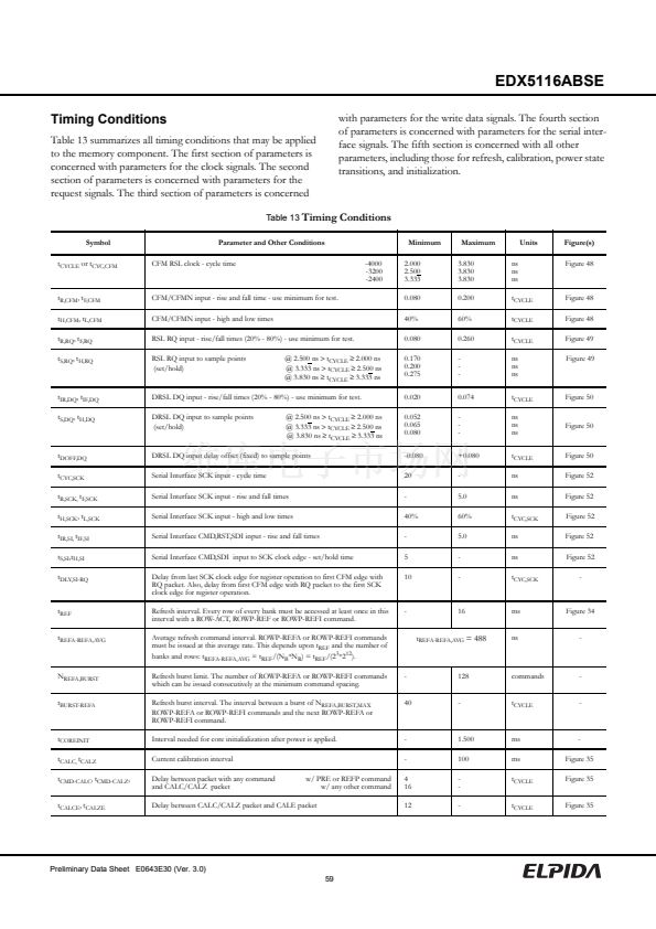
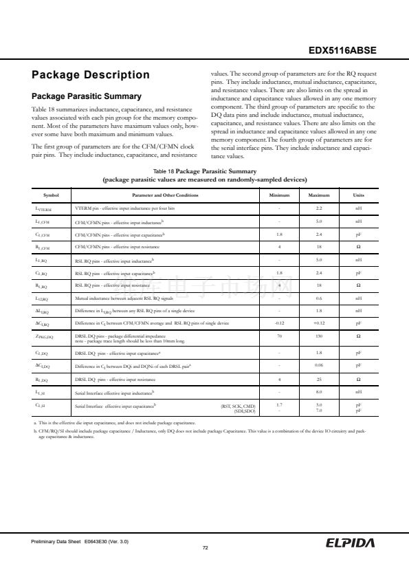
DRSL DQ input delay offset (fixed) to sample points
Serial Interface SCK input - cycle time
Serial Interface SCK input - rise and fall times
Serial Interface SCK input - high and low times
Serial Interface CMD,RST,SDI input - rise and fall times
Serial Interface CMD,SDI input to SCK clock edge - set/hold time
Delay from last SCK clock edge for register operation to first CFM edge with
RQ packet. Also, delay from first CFM edge with RQ packet to the first SCK
clock edge for register operation.
Refresh interval. Every row of every bank must be accessed at least once in this
interval with a ROW-ACT, ROWP-REF or ROWP-REFI command.
Average refresh command interval. ROWP-REFA or ROWP-REFI commands
must be issued at this average rate. This depends upon t
REF
and the number of
banks and rows: t
REFA-REFA,AVG
= t
REF
/(N
B
*N
R
) = t
REF
/(2
3
*2
12
).
Refresh burst limit. The number of ROWP-REFA or ROWP-REFI commands
which can be issued consecutively at the minimum command spacing.
Refresh burst interval. The interval between a burst of N
REFA,BURST,MAX
ROWP-REFA or ROWP-REFI commands and the next ROWP-REFA or
ROWP-REFI command.
Interval needed for core initialialization after power is applied.
Current calibration interval
Delay between packet with any command
and CALC/CALZ packet
w/ PRE or REFP command
w/ any other command
Figure 50
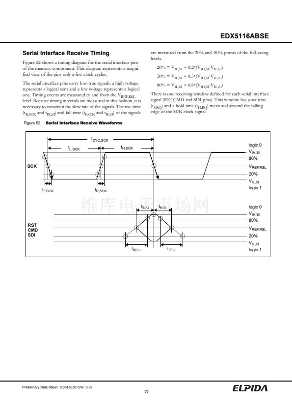
Figure 52
Figure 52
Figure 52
Figure 52
Figure 52
-
t
REF
t
REFA-REFA,AVG
-
16
t
REFA-REFA,AVG
= 488
ms
ns
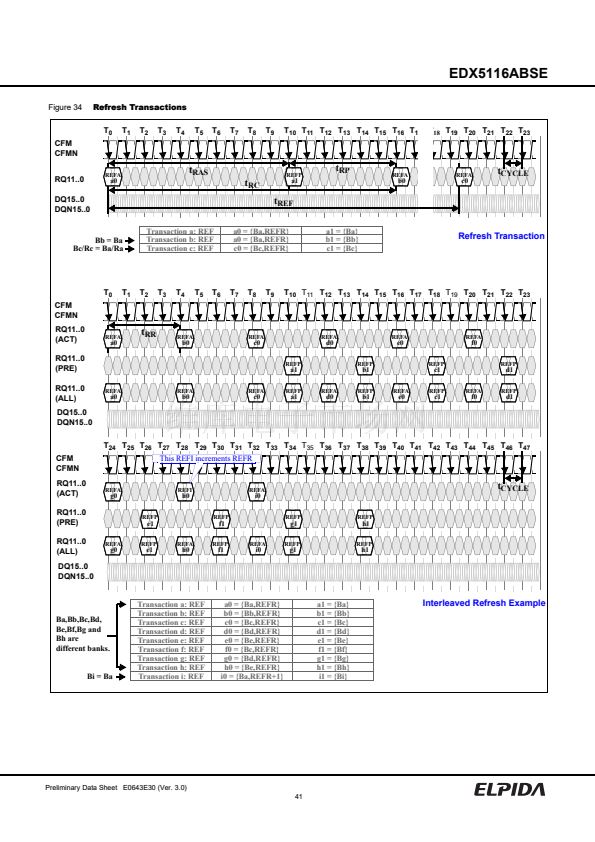
Figure 34
-
N
REFA,BURST
t
BURST-REFA
-
40
128
-
commands
t
CYCLE
-
-
t
COREINIT
t
CALC,
t
CALZ
t
CMD-CALC
, t
CMD-CALZ
,
t
CALCE
, t
CALZE
-
-
4
16
12
1.500
100
-
-
-
ms
ms
t
CYCLE
t
CYCLE
-
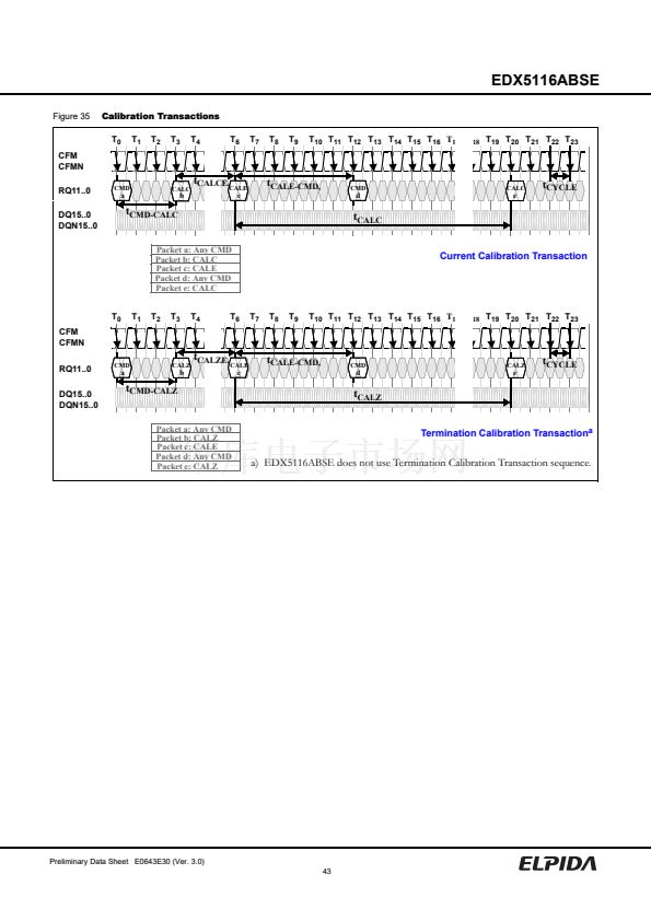
Figure 35
Figure 35
Figure 35
Delay between CALC/CALZ packet and CALE packet
Preliminary Data Sheet E0643E30 (Ver. 3.0)
59


 1
1
 2
2
 3
3
 4
4
 5
5
 6
6
 7
7
 8
8
 9
9
 10
10
 11
11
 12
12
 13
13
 14
14
 15
15
 16
16
 17
17
 18
18
 19
19
 20
20
 21
21
 22
22
 23
23
 24
24
 25
25
 26
26
 27
27
 28
28
 29
29
 30
30
 31
31
 32
32
 33
33
 34
34
 35
35
 36
36
 37
37
 38
38
 39
39
 40
40
 41
41
 42
42
 43
43
 44
44
 45
45
 46
46
 47
47
 48
48
 49
49
 50
50
 51
51
 52
52
 53
53
 54
54
 55
55
 56
56
 57
57
 58
58
 59
59
 60
60
 61
61
 62
62
 63
63
 64
64
 65
65
 66
66
 67
67
 68
68
 69
69
 70
70
 71
71
 72
72
 73
73
 74
74
 75
75
 76
76
 77
77
 78
78
