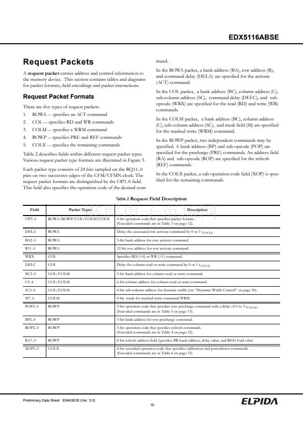
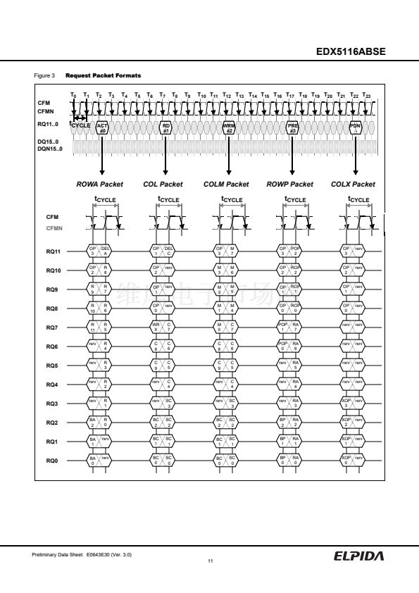
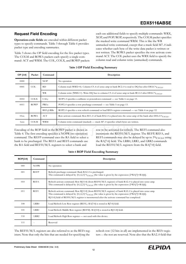
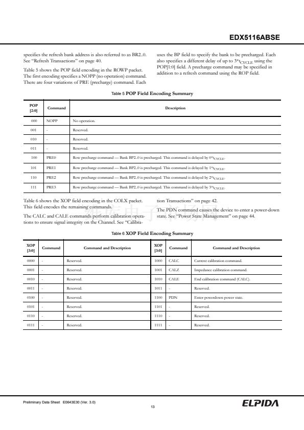
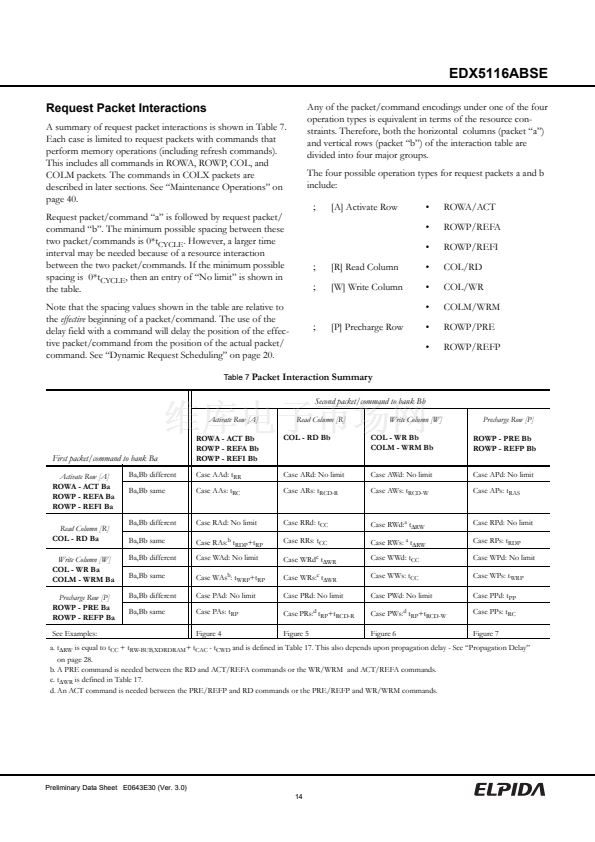
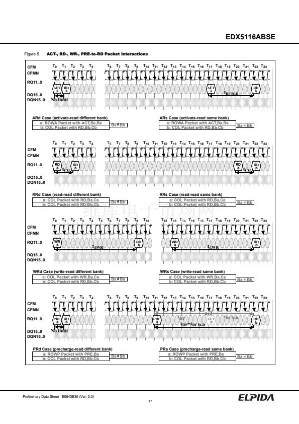
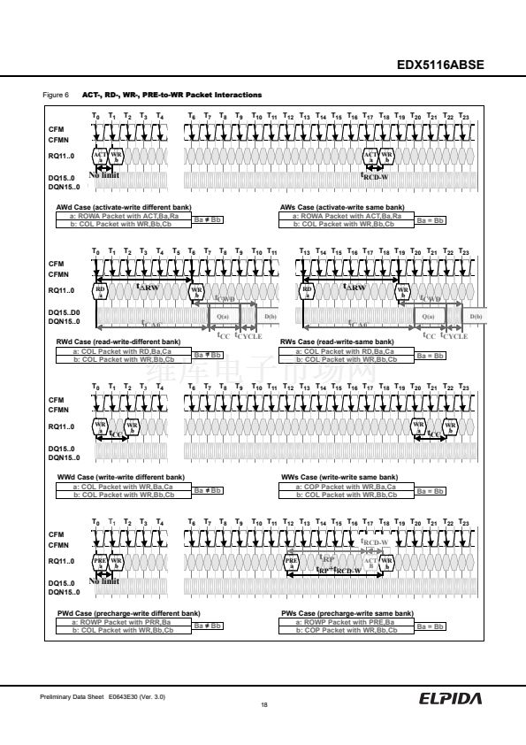
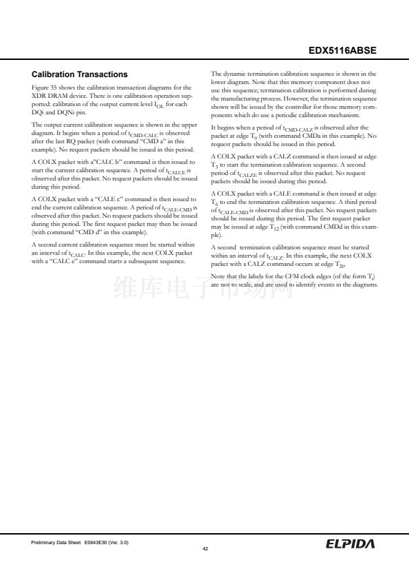
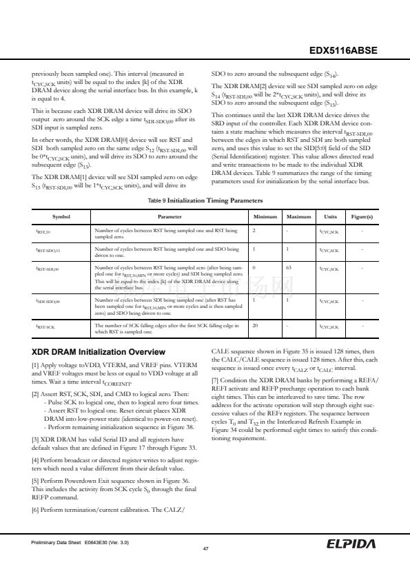
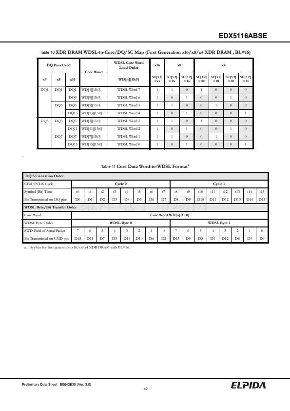
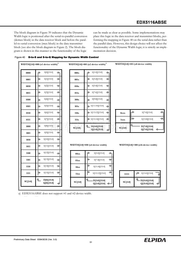
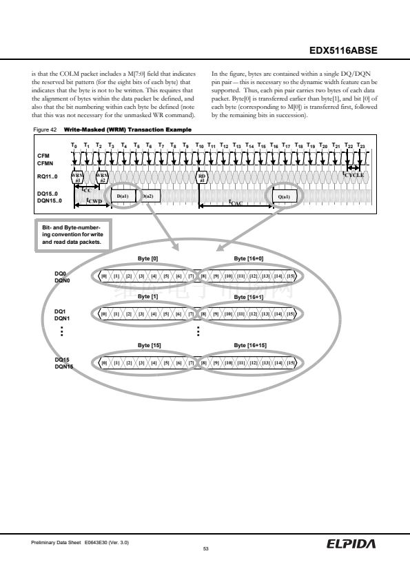
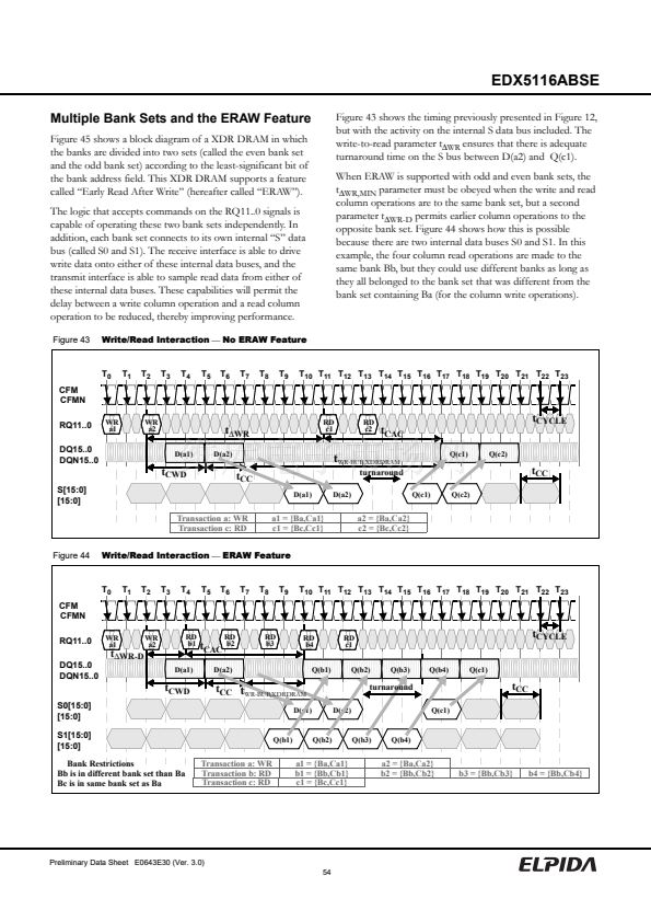
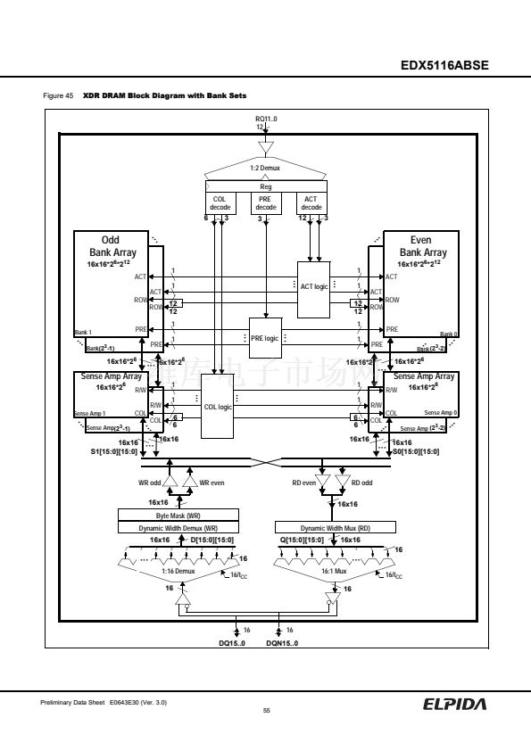
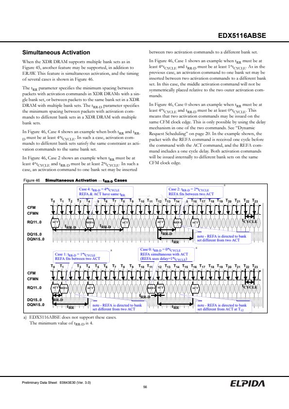
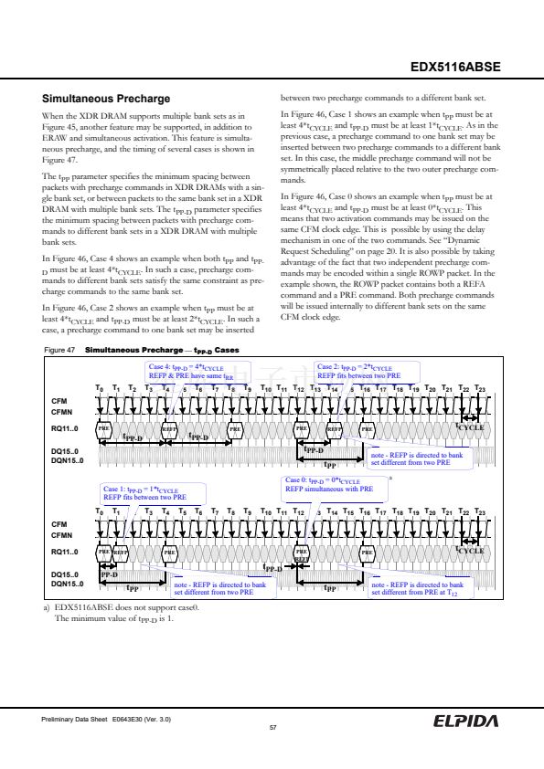
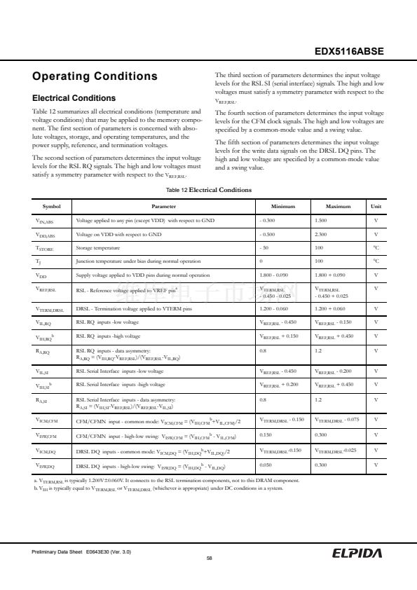
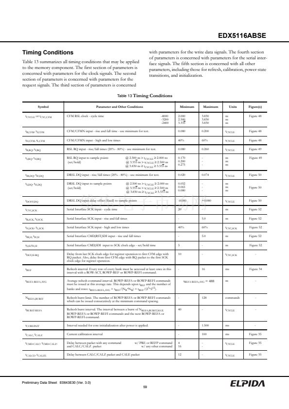
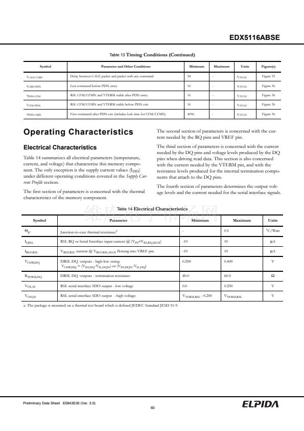
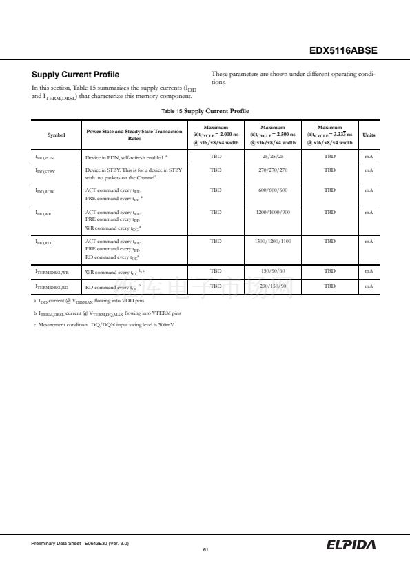
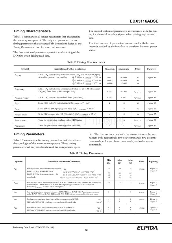
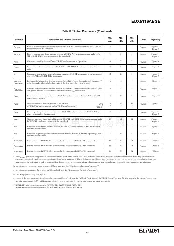
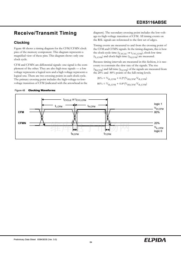
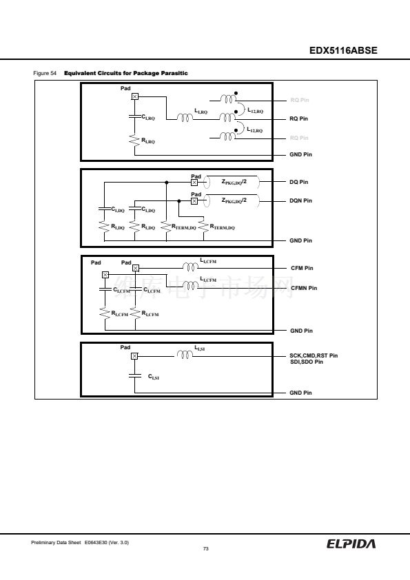
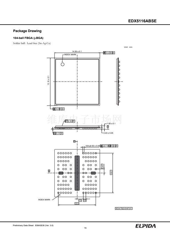
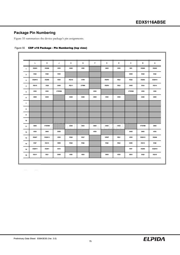
EDX5116ABSE
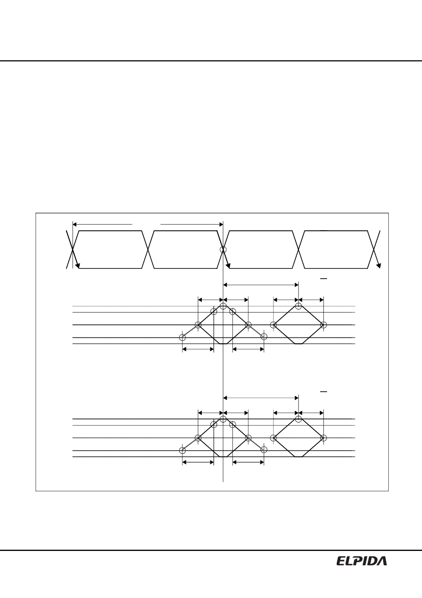
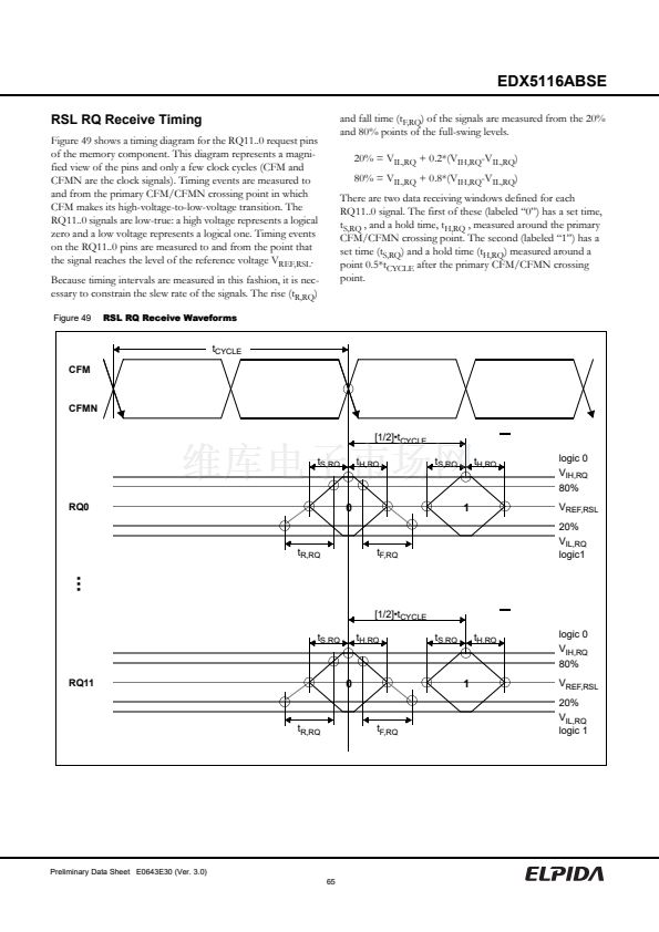
RSL RQ Receive Timing
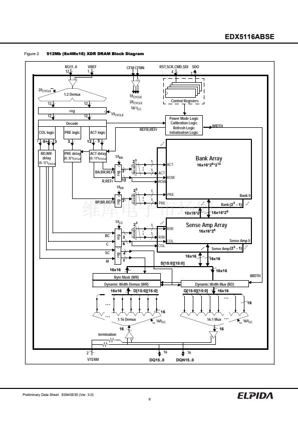
Figure 49 shows a timing diagram for the RQ11..0 request pins
of the memory component. This diagram represents a magni-
fied view of the pins and only a few clock cycles (CFM and
CFMN are the clock signals). Timing events are measured to
and from the primary CFM/CFMN crossing point in which
CFM makes its high-voltage-to-low-voltage transition. The
RQ11..0 signals are low-true: a high voltage represents a logical
zero and a low voltage represents a logical one. Timing events
on the RQ11..0 pins are measured to and from the point that
the signal reaches the level of the reference voltage V
REF,RSL
.
Because timing intervals are measured in this fashion, it is nec-
essary to constrain the slew rate of the signals. The rise (t
R,RQ
)
Figure 49
RSL RQ Receive Waveforms
and fall time (t
F,RQ
) of the signals are measured from the 20%
and 80% points of the full-swing levels.
20% = V
IL,RQ
+ 0.2*(V
IH,RQ
-V
IL,RQ
)
80% = V
IL,RQ
+ 0.8*(V
IH,RQ
-V
IL,RQ
)
There are two data receiving windows defined for each
RQ11..0 signal. The first of these (labeled 鈥?鈥? has a set time,
t
S,RQ
, and a hold time, t
H,RQ
, measured around the primary
CFM/CFMN crossing point. The second (labeled 鈥?鈥? has a
set time (t
S,RQ
) and a hold time (t
H,RQ
) measured around a
point 0.5*t
CYCLE
after the primary CFM/CFMN crossing
point.
t
CYCLE
CFM
CFMN
[1/2]鈥
CYCLE
t
S,RQ
t
H,RQ
t
S,RQ
t
H,RQ
logic 0
V
IH,RQ
80%
V
REF,RSL
20%
V
IL,RQ
logic1
RQ0
0
1
t
R,RQ
t
F,RQ
...
[1/2]鈥
CYCLE
t
S,RQ
t
H,RQ
t
S,RQ
t
H,RQ
logic 0
V
IH,RQ
80%
V
REF,RSL
20%
V
IL,RQ
logic 1
RQ11
0
1
t
R,RQ
t
F,RQ
Preliminary Data Sheet E0643E30 (Ver. 3.0)
65


 1
1
 2
2
 3
3
 4
4
 5
5
 6
6
 7
7
 8
8
 9
9
 10
10
 11
11
 12
12
 13
13
 14
14
 15
15
 16
16
 17
17
 18
18
 19
19
 20
20
 21
21
 22
22
 23
23
 24
24
 25
25
 26
26
 27
27
 28
28
 29
29
 30
30
 31
31
 32
32
 33
33
 34
34
 35
35
 36
36
 37
37
 38
38
 39
39
 40
40
 41
41
 42
42
 43
43
 44
44
 45
45
 46
46
 47
47
 48
48
 49
49
 50
50
 51
51
 52
52
 53
53
 54
54
 55
55
 56
56
 57
57
 58
58
 59
59
 60
60
 61
61
 62
62
 63
63
 64
64
 65
65
 66
66
 67
67
 68
68
 69
69
 70
70
 71
71
 72
72
 73
73
 74
74
 75
75
 76
76
 77
77
 78
78
