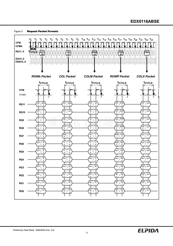
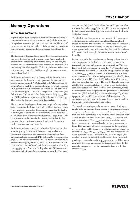
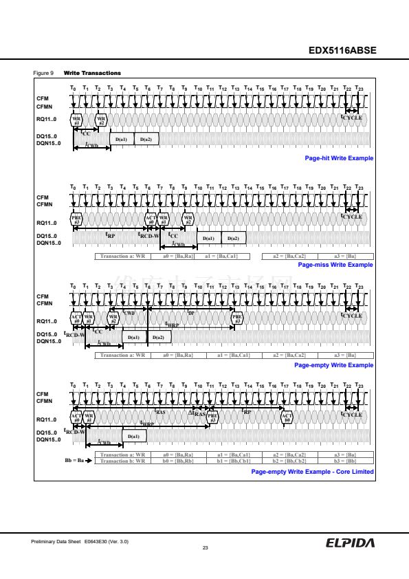
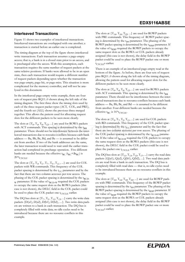
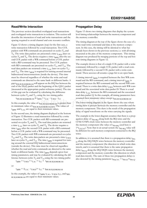
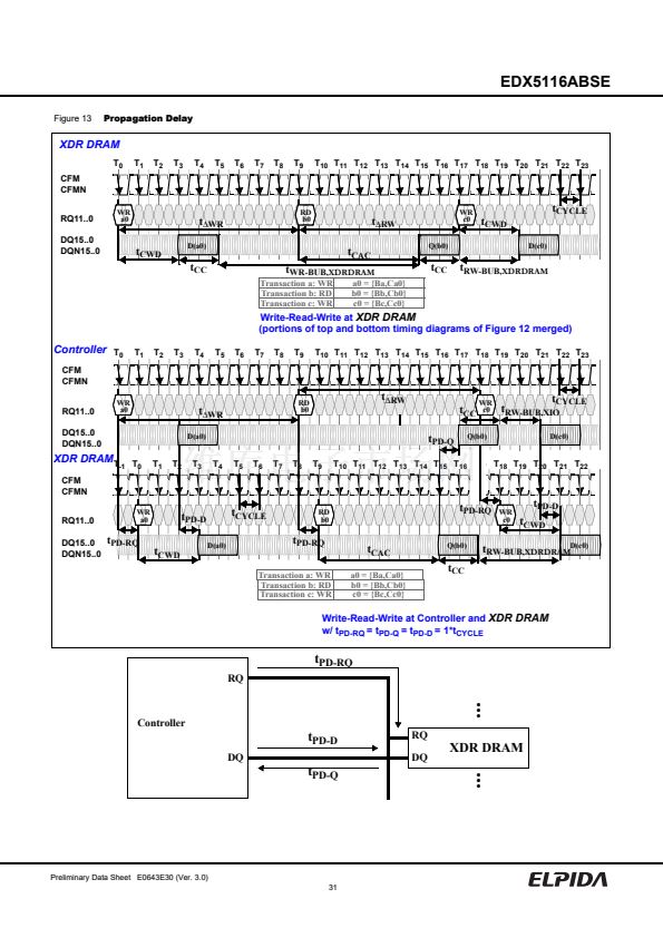
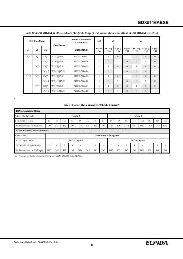
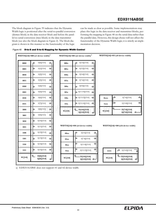
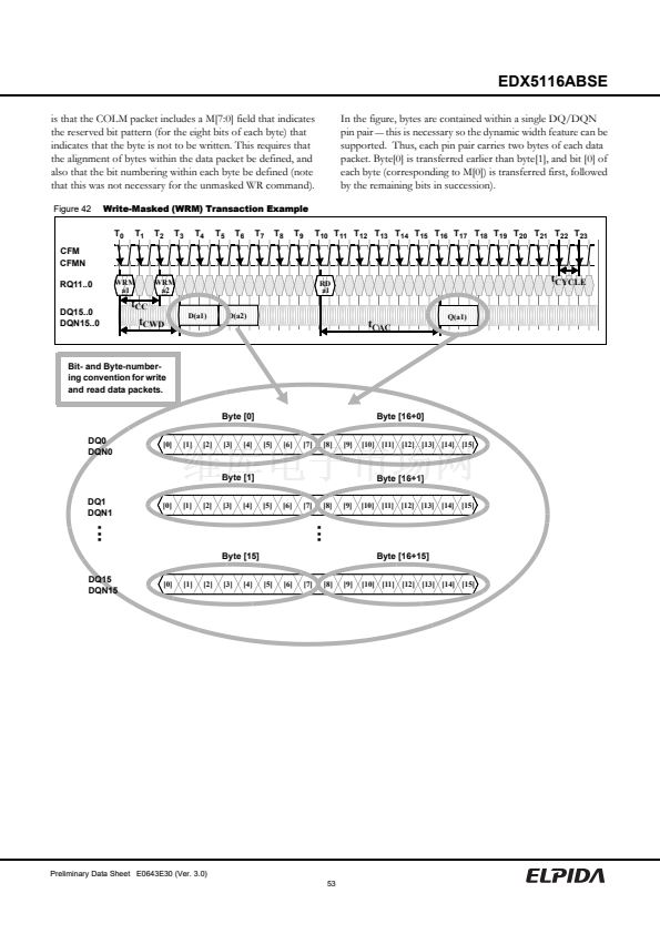
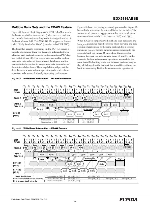
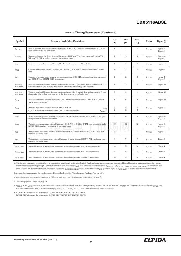
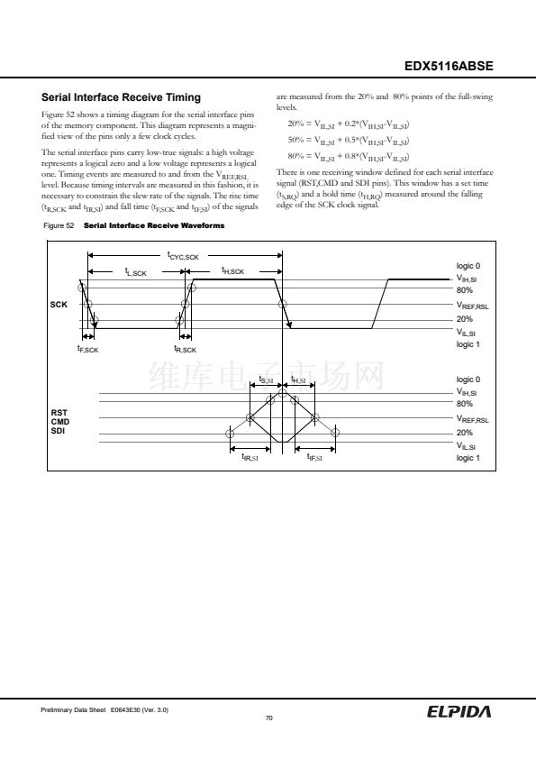
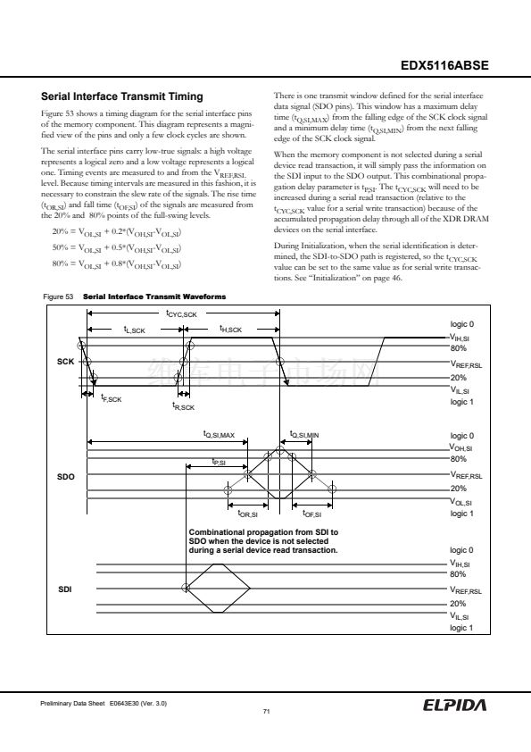
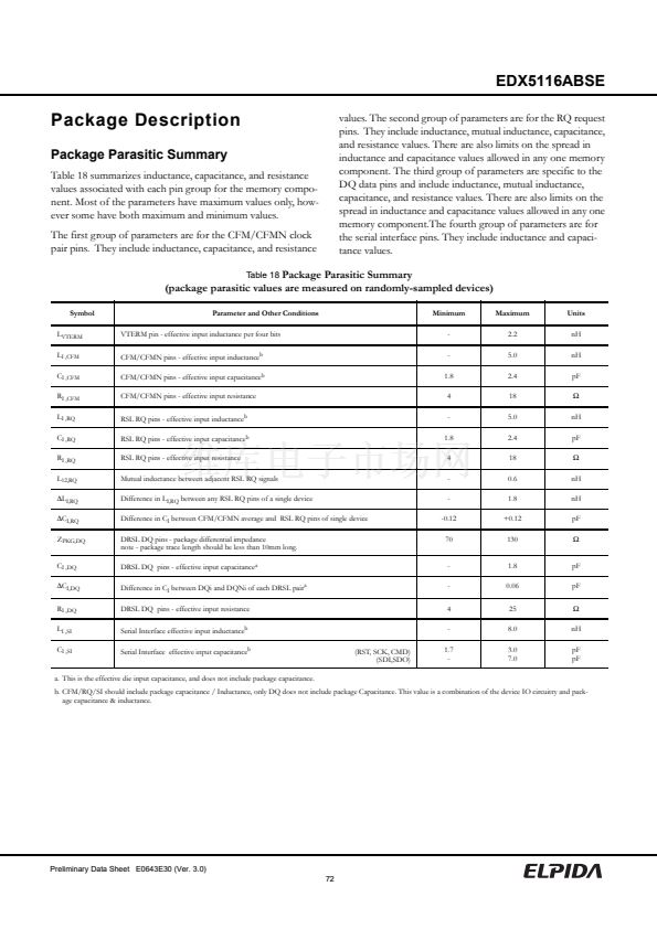
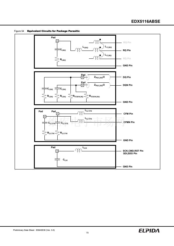
EDX5116ABSE
Block Diagram
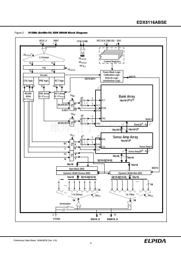
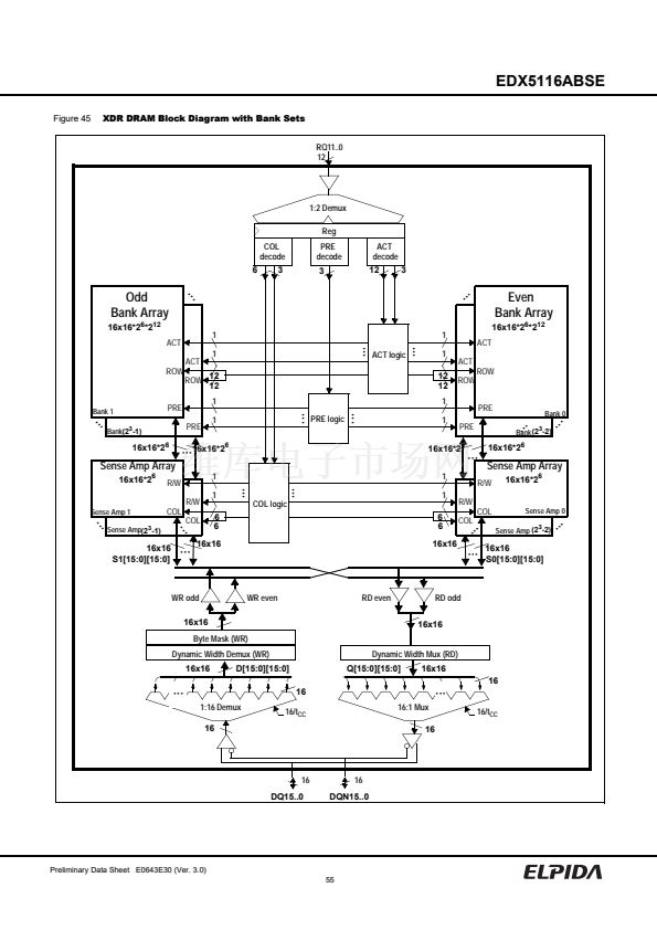
A block diagram of the XDR DRAM device is shown in
Figure 2. It shows all interface pins and major internal blocks.
The CFM and CFMN clock signals are received and used by
the clock generation logic to produce three virtual clock sig-
nals: 1/t
CYCLE
, 2/t
CYCLE
, and 16/t
CC
. The frequency of these
signals are 1x, 2x, and 8x that of the CFM and CFMN signals.
These virtual signals show the effective data rate of the logic
blocks to which they connect; they are not necessarily present
in the actual memory component.
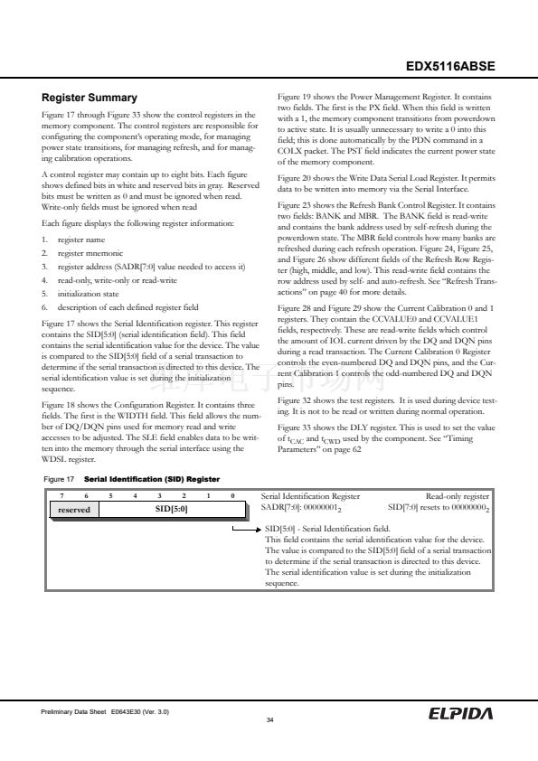
The RQ11..0 pins receive the request packet. Two 12-bit words
are received in one t
CYCLE
interval. This is indicated by the 2/
t
CYCLE
clocking signal connected to the 1:2 Demux Block that
assembles the 24-bit request packet. These 24 bits are loaded
into a register (clocked by the 1/t
CYCLE
clocking signal) and
decoded by the Decode Block. The VREF pin supplies a refer-
ence voltage used by the RQ receivers.
Three sets of control signals are produced by the Decode
Block. These include the bank (BA) and row (R) addresses for
an activate (ACT) command, the bank (BR) and row (REFr)
addresses for a refresh activate (REFA) command, the bank
(BP) address for a precharge (PRE) command, the bank (BR)
address for a refresh precharge (REFP) command, and the
bank (BC) and column (C and SC) addresses for a read (RD) or
write (WR or WRM) command. In addition, a mask (M) is used
for a masked write (WRM) command.
These commands can all be optionally delayed in increments of
t
CYCLE
under control of delay fields in the request. The control
signals of the commands are loaded into registers and pre-
sented to the memory core. These registers are clocked at max-
imum rates determined by core timing parameters, in this case
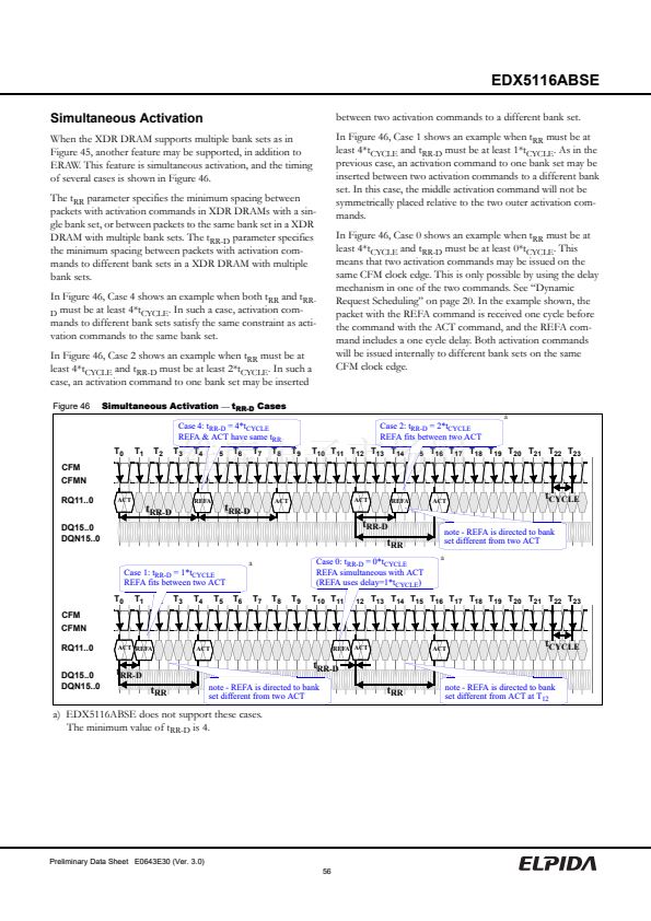
1/t
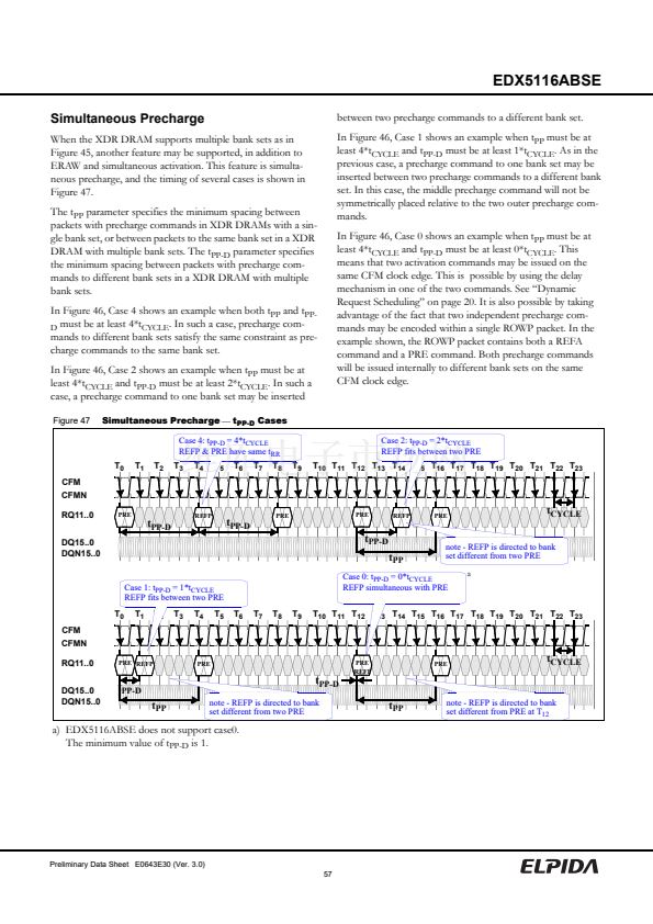
RR
, 1/t
PP
, and 1/t
CC
(1/4, 1/4, and 1/2 the frequency of
CFM in the -3200 component). These registers may be loaded
at any t
CYCLE
rising edge. Once loaded, they should not be
changed until a t
RR
, t
PP
, or t
CC
time later because timing paths
of the memory core need time to settle.
A bank address is decoded for an ACT command. The indi-
cated row of the selected bank is sensed and placed into the
associated sense amp array for the bank. Sensing a row is also
referred to as 鈥渙pening a page鈥?for the bank.
Another bank address is decoded for a PRE command. The
indicated bank and associated sense amp array are precharged
to a state in which a subsequent ACT command can be
applied. Precharging a bank is also called 鈥渃losing the page鈥?for
the bank.
After a bank is given an ACT command and before it is given a
PRE command, it may receive read (RD) and write (WR) col-
umn commands. These commands permit the data in the
bank鈥檚 associated sense amp array to be accessed.
For a WR command, the bank address is decoded. The indi-
cated column of the associated sense amp array of the selected
bank is written with the data received from the DQ15..0 pins.
The bank address is decoded for a RD command. The indi-
cated column of the selected bank鈥檚 associated sense amp array
is read. The data is transmitted onto the DQ15..0 pins.
The DQ15..0 pins receive the write data packet (D) for a write
transaction. 16 sixteen-bit words are received in one t
CC
inter-
val. This is indicated by the 16/t
CC
clocking signal connected
to the 1:16 Demux Block that assembles the 16x16-bit write
data packet. The write data is then driven to the selected Sense
Amp Array Bank.
16 sixteen-bit words are accessed in the selected Sense Amp
Array Bank for a read transaction. The DQ15..0 pins transmit
this read data packet (Q) in one t
CC
interval. This is indicated
by the 16/t
CC
clocking signal connected to the 16:1 Mux
Block. The VTERM pin supplies a termination voltage for the
DQ pins.
The RST, SCK, and CMD pins connect to the Control Register
block. These pins supply the data, address, and control needed
to write the control registers. The read data for the these regis-
ters is accessed through the SDO/SDI pins. These pins are
also used to initialize the device.
The control registers are used to transition between power
modes, and are also used for calibrating the high speed trans-
mit and receive circuits of the device. The control registers also
supply bank (REFB) and row (REFr) addresses for refresh
operations.
Preliminary Data Sheet E0643E30 (Ver. 3.0)
8


 1
1
 2
2
 3
3
 4
4
 5
5
 6
6
 7
7
 8
8
 9
9
 10
10
 11
11
 12
12
 13
13
 14
14
 15
15
 16
16
 17
17
 18
18
 19
19
 20
20
 21
21
 22
22
 23
23
 24
24
 25
25
 26
26
 27
27
 28
28
 29
29
 30
30
 31
31
 32
32
 33
33
 34
34
 35
35
 36
36
 37
37
 38
38
 39
39
 40
40
 41
41
 42
42
 43
43
 44
44
 45
45
 46
46
 47
47
 48
48
 49
49
 50
50
 51
51
 52
52
 53
53
 54
54
 55
55
 56
56
 57
57
 58
58
 59
59
 60
60
 61
61
 62
62
 63
63
 64
64
 65
65
 66
66
 67
67
 68
68
 69
69
 70
70
 71
71
 72
72
 73
73
 74
74
 75
75
 76
76
 77
77
 78
78
