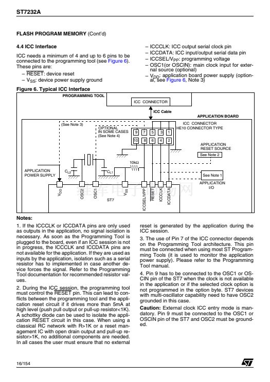
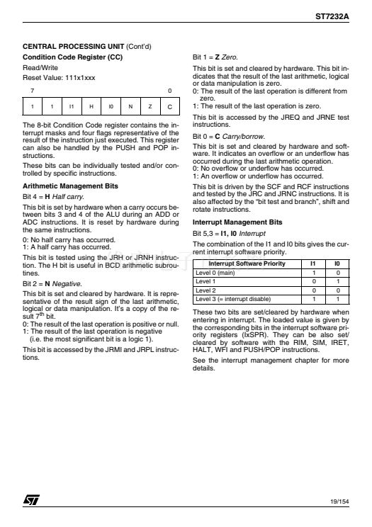
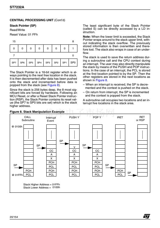
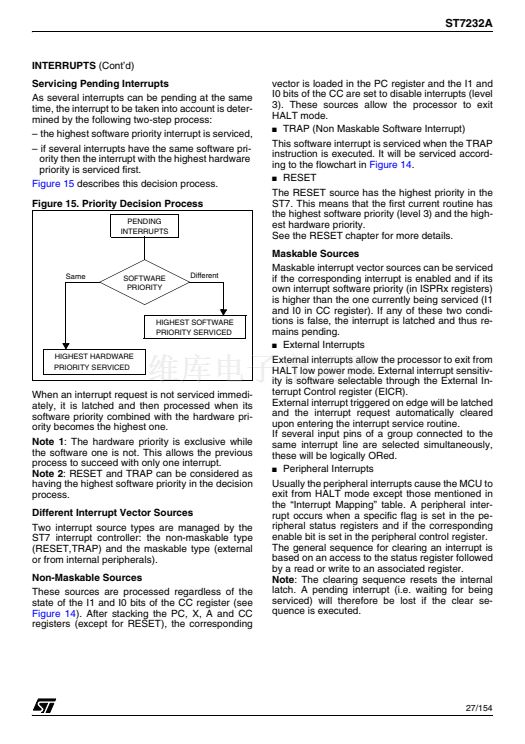
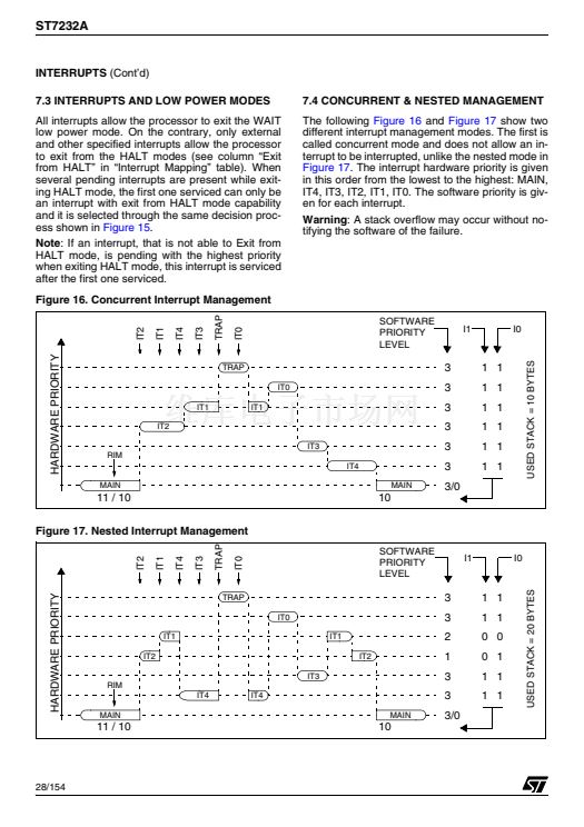
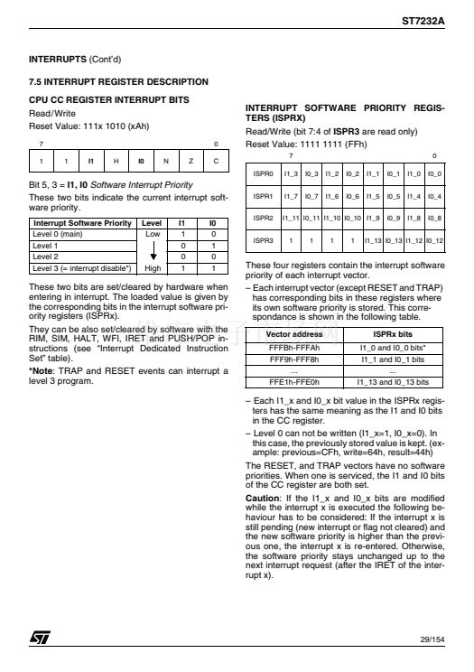
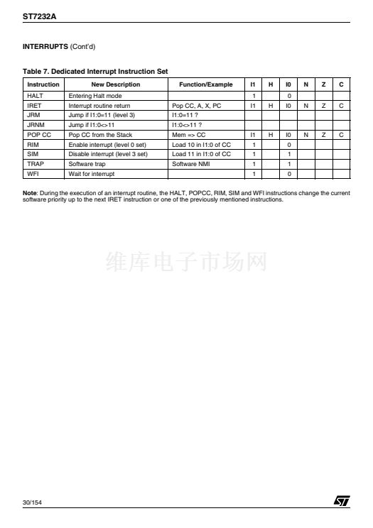
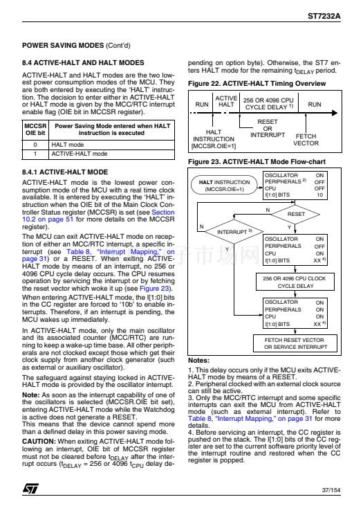
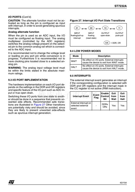
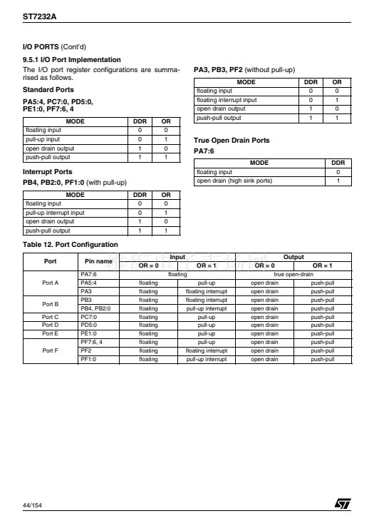
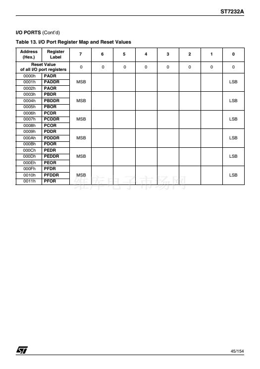
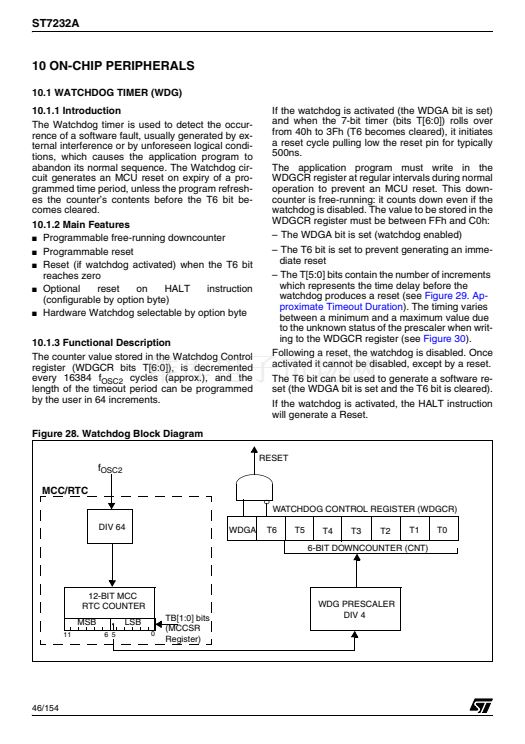
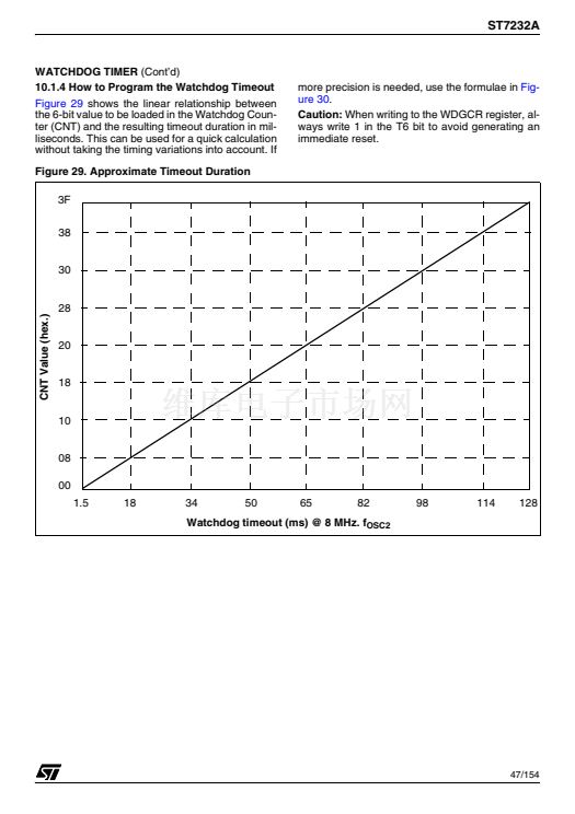
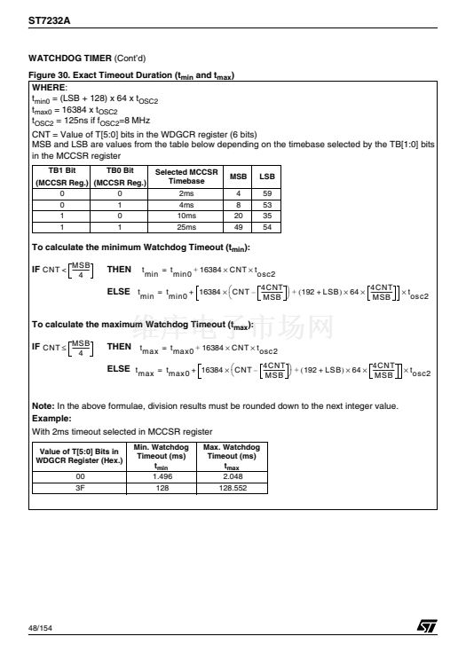
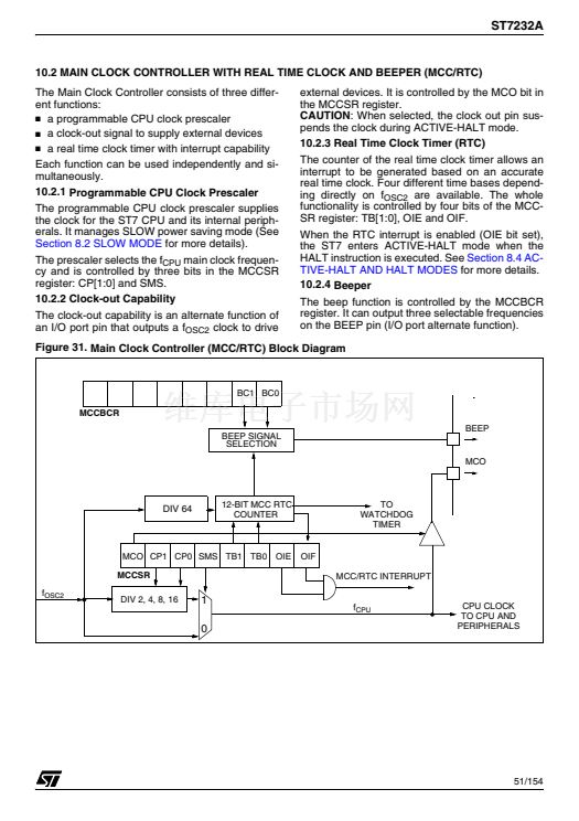
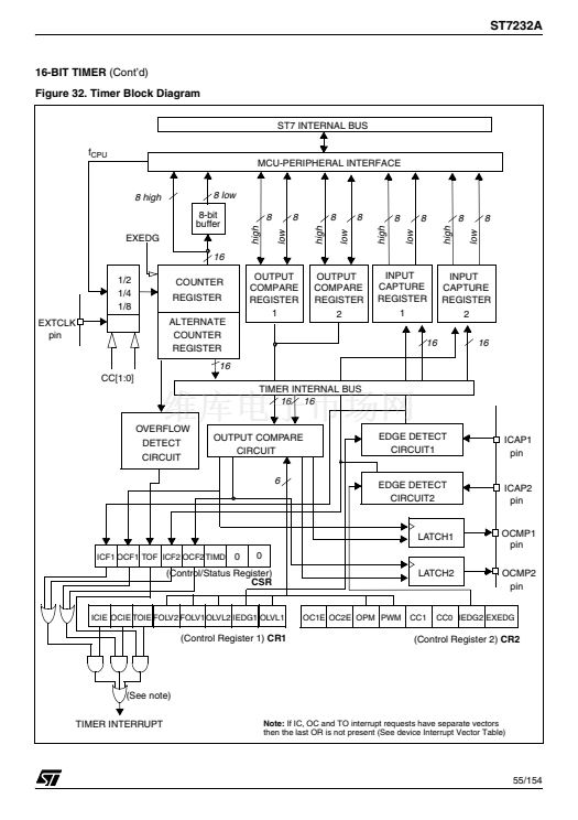
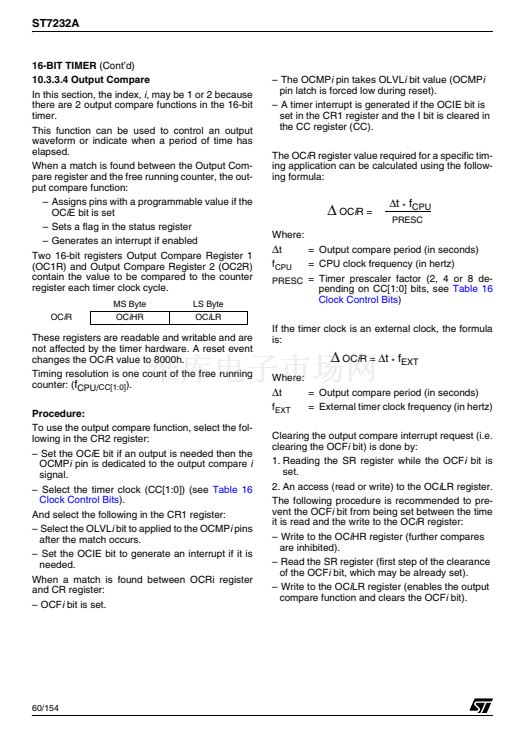
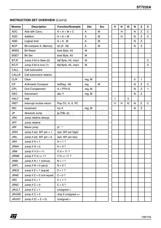
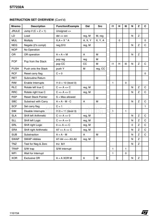
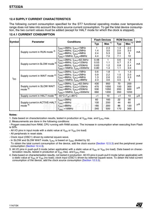
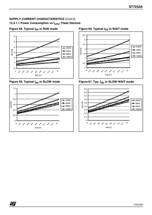
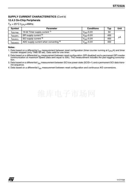
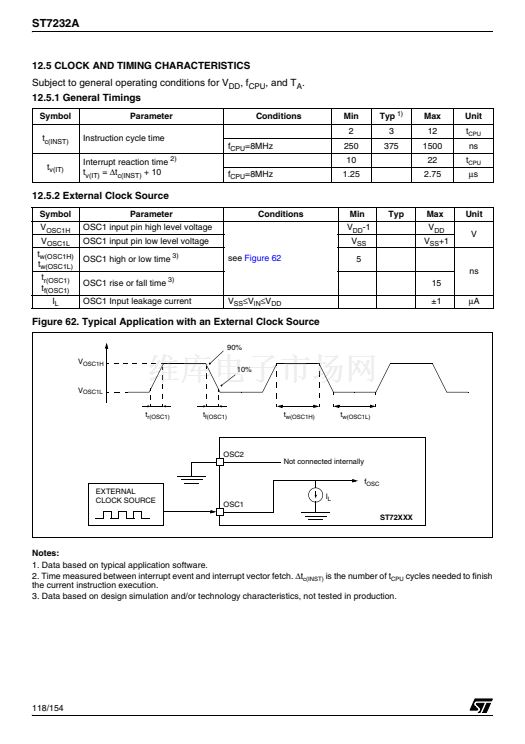
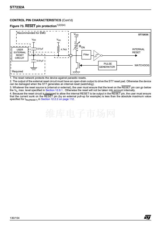
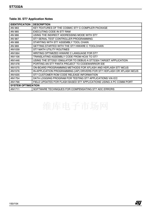
ST7232A
16-BIT TIMER
(Cont鈥檇)
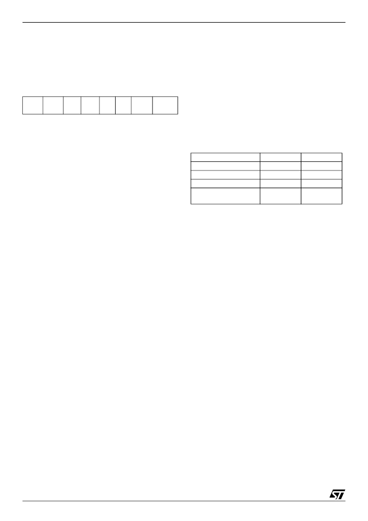
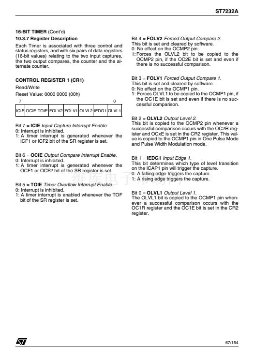
CONTROL REGISTER 2 (CR2)
Read/Write
Reset Value: 0000 0000 (00h)
7
0
OC1E OC2E OPM PWM CC1 CC0 IEDG2 EXEDG
Bit 4 =
PWM
Pulse Width Modulation.
0: PWM mode is not active.
1: PWM mode is active, the OCMP1 pin outputs a
programmable cyclic signal; the length of the
pulse depends on the value of OC1R register;
the period depends on the value of OC2R regis-
ter.
Bit 3, 2 =
CC[1:0]
Clock Control.
The timer clock mode depends on these bits:
Table 16. Clock Control Bits
Timer Clock
f
CPU
/ 4
f
CPU
/ 2
f
CPU
/ 8
External Clock (where
available)
CC1
0
0
1
1
CC0
0
1
0
1
Bit 7 =
OC1E
Output Compare 1 Pin Enable.
This bit is used only to output the signal from the
timer on the OCMP1 pin (OLV1 in Output Com-
pare mode, both OLV1 and OLV2 in PWM and
one-pulse mode). Whatever the value of the OC1E
bit, the Output Compare 1 function of the timer re-
mains active.
0: OCMP1 pin alternate function disabled (I/O pin
free for general-purpose I/O).
1: OCMP1 pin alternate function enabled.
Bit 6 =
OC2E
Output Compare 2 Pin Enable.
This bit is used only to output the signal from the
timer on the OCMP2 pin (OLV2 in Output Com-
pare mode). Whatever the value of the OC2E bit,
the Output Compare 2 function of the timer re-
mains active.
0: OCMP2 pin alternate function disabled (I/O pin
free for general-purpose I/O).
1: OCMP2 pin alternate function enabled.
Bit 5 =
OPM
One Pulse Mode.
0: One Pulse Mode is not active.
1: One Pulse Mode is active, the ICAP1 pin can be
used to trigger one pulse on the OCMP1 pin; the
active transition is given by the IEDG1 bit. The
length of the generated pulse depends on the
contents of the OC1R register.
Note:
If the external clock pin is not available, pro-
gramming the external clock configuration stops
the counter.
Bit 1 =
IEDG2
Input Edge 2.
This bit determines which type of level transition
on the ICAP2 pin will trigger the capture.
0: A falling edge triggers the capture.
1: A rising edge triggers the capture.
Bit 0 =
EXEDG
External Clock Edge.
This bit determines which type of level transition
on the external clock pin EXTCLK will trigger the
counter register.
0: A falling edge triggers the counter register.
1: A rising edge triggers the counter register.
68/154
1


 1
1
 2
2
 3
3
 4
4
 5
5
 6
6
 7
7
 8
8
 9
9
 10
10
 11
11
 12
12
 13
13
 14
14
 15
15
 16
16
 17
17
 18
18
 19
19
 20
20
 21
21
 22
22
 23
23
 24
24
 25
25
 26
26
 27
27
 28
28
 29
29
 30
30
 31
31
 32
32
 33
33
 34
34
 35
35
 36
36
 37
37
 38
38
 39
39
 40
40
 41
41
 42
42
 43
43
 44
44
 45
45
 46
46
 47
47
 48
48
 49
49
 50
50
 51
51
 52
52
 53
53
 54
54
 55
55
 56
56
 57
57
 58
58
 59
59
 60
60
 61
61
 62
62
 63
63
 64
64
 65
65
 66
66
 67
67
 68
68
 69
69
 70
70
 71
71
 72
72
 73
73
 74
74
 75
75
 76
76
 77
77
 78
78
 79
79
 80
80
 81
81
 82
82
 83
83
 84
84
 85
85
 86
86
 87
87
 88
88
 89
89
 90
90
 91
91
 92
92
 93
93
 94
94
 95
95
 96
96
 97
97
 98
98
 99
99
 100
100
 101
101
 102
102
 103
103
 104
104
 105
105
 106
106
 107
107
 108
108
 109
109
 110
110
 111
111
 112
112
 113
113
 114
114
 115
115
 116
116
 117
117
 118
118
 119
119
 120
120
 121
121
 122
122
 123
123
 124
124
 125
125
 126
126
 127
127
 128
128
 129
129
 130
130
 131
131
 132
132
 133
133
 134
134
 135
135
 136
136
 137
137
 138
138
 139
139
 140
140
 141
141
 142
142
 143
143
 144
144
 145
145
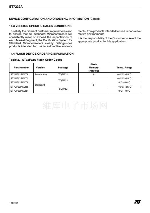 146
146
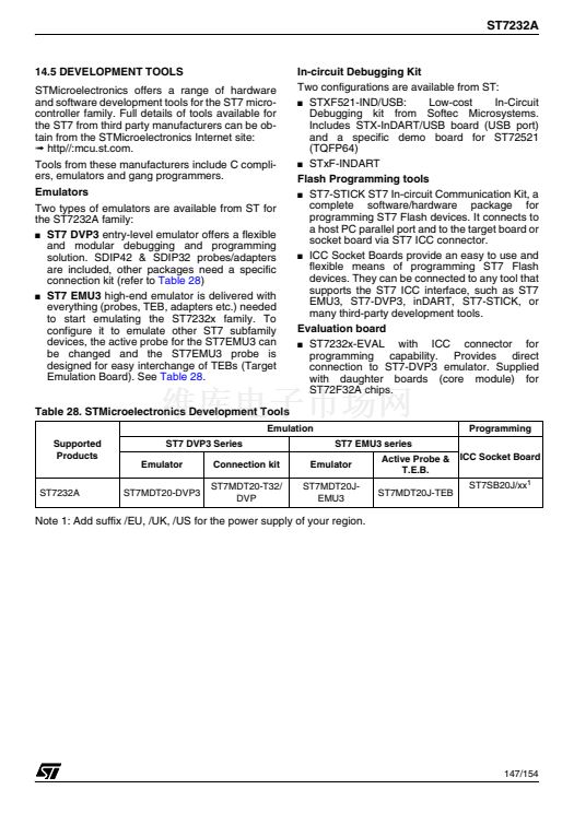 147
147
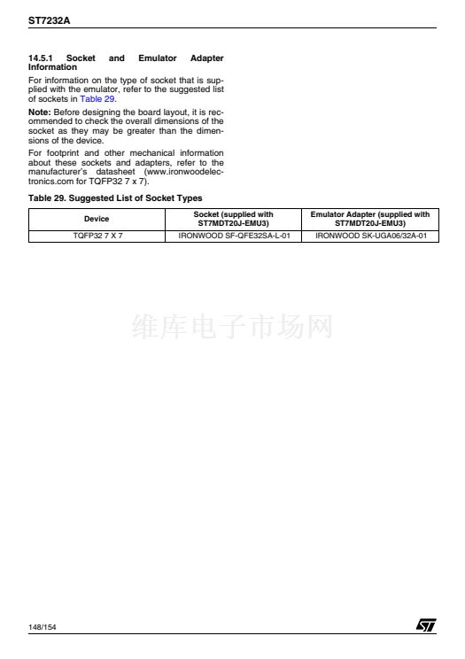 148
148
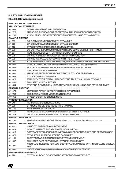 149
149
 150
150
 151
151
 152
152
 153
153
 154
154
