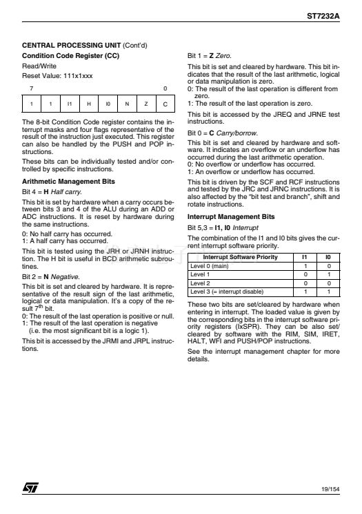
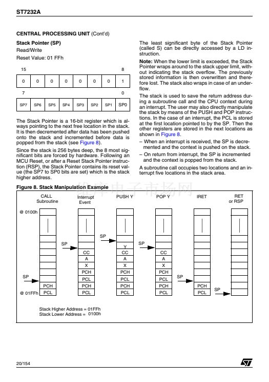
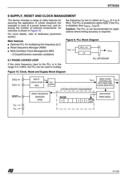
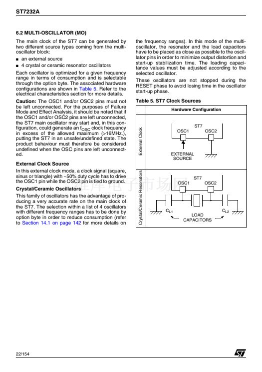
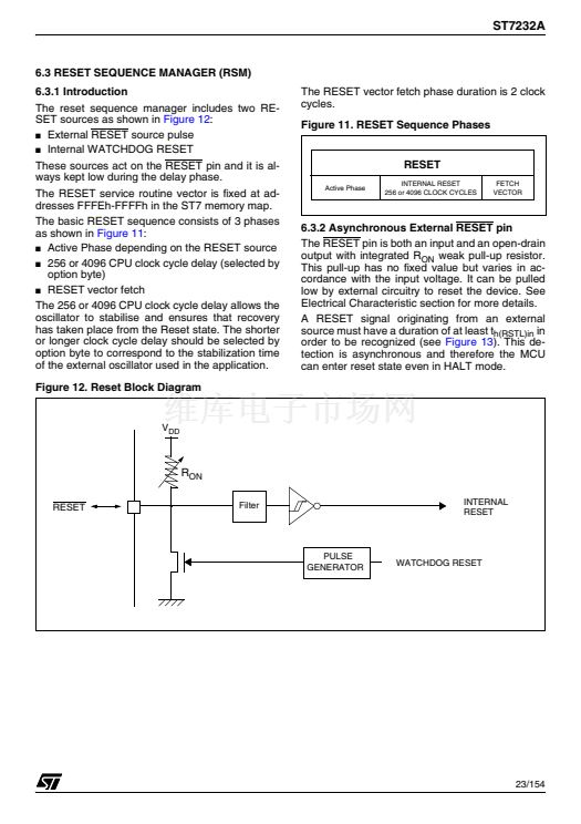
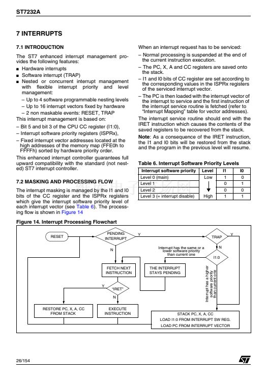
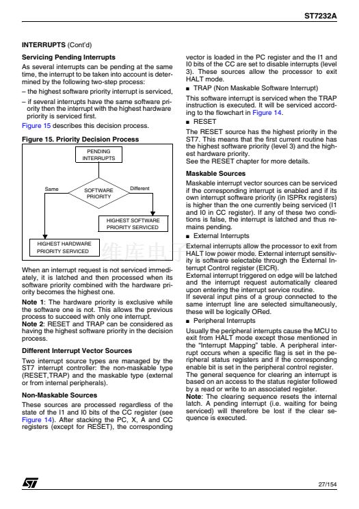
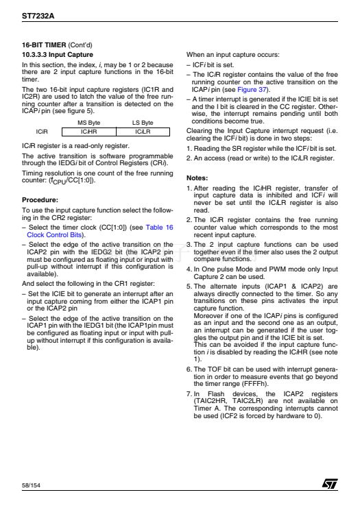
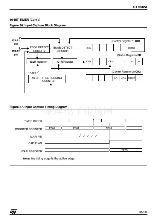
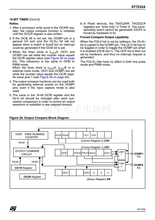
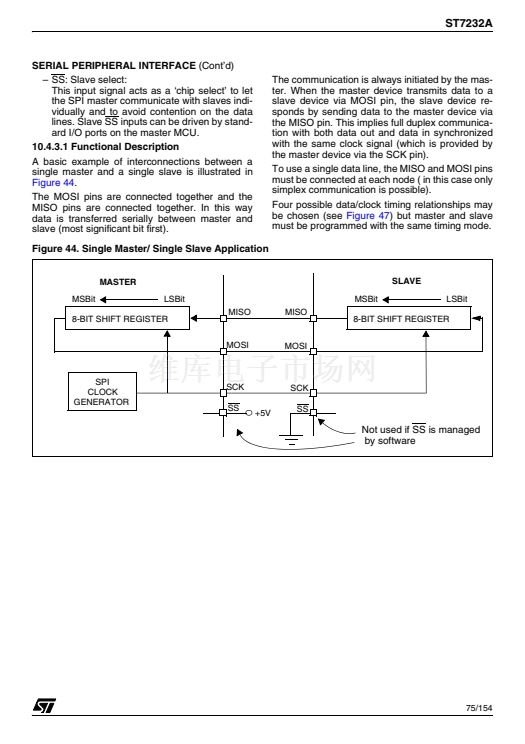
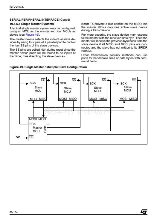
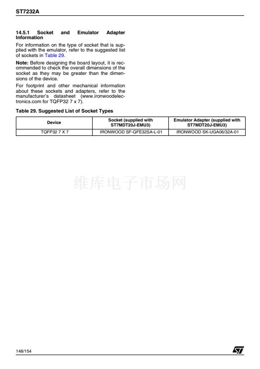
ST7232A
SERIAL COMMUNICATIONS INTERFACE
(Cont鈥檇)
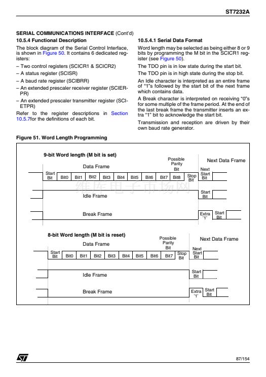
10.5.4 Functional Description
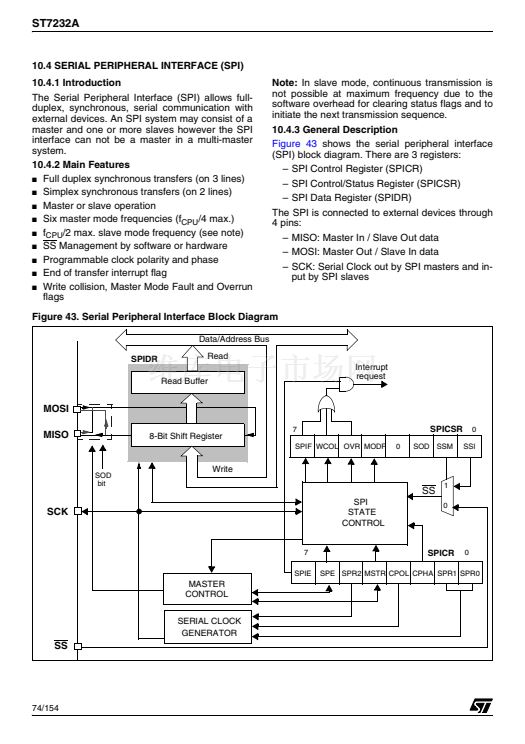
The block diagram of the Serial Control Interface,
is shown in
Figure 50.
It contains 6 dedicated reg-
isters:
鈥?Two control registers (SCICR1 & SCICR2)
鈥?A status register (SCISR)
鈥?A baud rate register (SCIBRR)
鈥?An extended prescaler receiver register (SCIER-
PR)
鈥?An extended prescaler transmitter register (SCI-
ETPR)
Refer to the register descriptions in
Section
10.5.7for
the definitions of each bit.
10.5.4.1 Serial Data Format
Word length may be selected as being either 8 or 9
bits by programming the M bit in the SCICR1 reg-
ister (see
Figure 50).
The TDO pin is in low state during the start bit.
The TDO pin is in high state during the stop bit.
An Idle character is interpreted as an entire frame
of 鈥?鈥漵 followed by the start bit of the next frame
which contains data.
A Break character is interpreted on receiving 鈥?鈥漵
for some multiple of the frame period. At the end of
the last break frame the transmitter inserts an ex-
tra 鈥?鈥?bit to acknowledge the start bit.
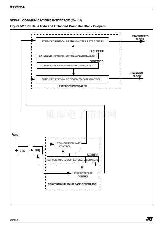
Transmission and reception are driven by their
own baud rate generator.
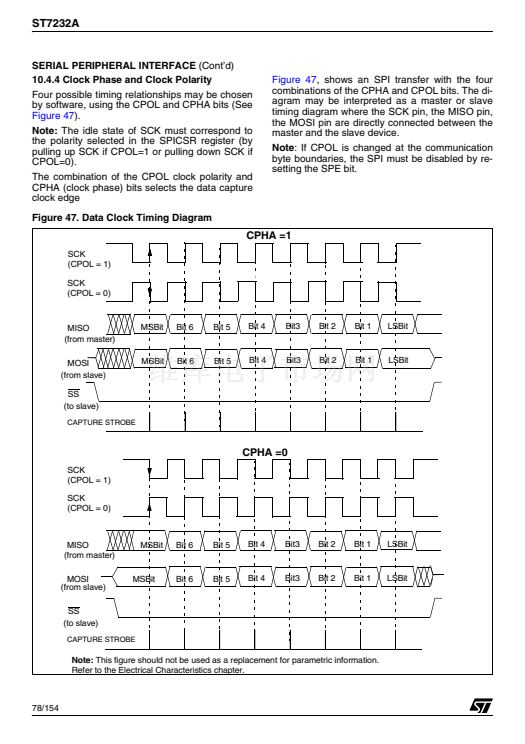
Figure 51. Word Length Programming
9-bit Word length (M bit is set)
Data Frame
Start
Bit
Bit0
Bit1
Bit2
Bit3
Bit4
Bit5
Bit6
Bit7
Possible
Parity
Bit
Bit8
Next Data Frame
Next
Stop Start
Bit
Bit
Start
Bit
Idle Frame
Break Frame
Extra
鈥?鈥?/div>
Start
Bit
8-bit Word length (M bit is reset)
Data Frame
Start
Bit
Bit0
Bit1
Bit2
Bit3
Bit4
Bit5
Bit6
Possible
Parity
Bit
Bit7
Stop
Bit
Next Data Frame
Next
Start
Bit
Start
Bit
Extra Start
Bit
鈥?鈥?/div>
Idle Frame
Break Frame
87/154
1


 1
1
 2
2
 3
3
 4
4
 5
5
 6
6
 7
7
 8
8
 9
9
 10
10
 11
11
 12
12
 13
13
 14
14
 15
15
 16
16
 17
17
 18
18
 19
19
 20
20
 21
21
 22
22
 23
23
 24
24
 25
25
 26
26
 27
27
 28
28
 29
29
 30
30
 31
31
 32
32
 33
33
 34
34
 35
35
 36
36
 37
37
 38
38
 39
39
 40
40
 41
41
 42
42
 43
43
 44
44
 45
45
 46
46
 47
47
 48
48
 49
49
 50
50
 51
51
 52
52
 53
53
 54
54
 55
55
 56
56
 57
57
 58
58
 59
59
 60
60
 61
61
 62
62
 63
63
 64
64
 65
65
 66
66
 67
67
 68
68
 69
69
 70
70
 71
71
 72
72
 73
73
 74
74
 75
75
 76
76
 77
77
 78
78
 79
79
 80
80
 81
81
 82
82
 83
83
 84
84
 85
85
 86
86
 87
87
 88
88
 89
89
 90
90
 91
91
 92
92
 93
93
 94
94
 95
95
 96
96
 97
97
 98
98
 99
99
 100
100
 101
101
 102
102
 103
103
 104
104
 105
105
 106
106
 107
107
 108
108
 109
109
 110
110
 111
111
 112
112
 113
113
 114
114
 115
115
 116
116
 117
117
 118
118
 119
119
 120
120
 121
121
 122
122
 123
123
 124
124
 125
125
 126
126
 127
127
 128
128
 129
129
 130
130
 131
131
 132
132
 133
133
 134
134
 135
135
 136
136
 137
137
 138
138
 139
139
 140
140
 141
141
 142
142
 143
143
 144
144
 145
145
 146
146
 147
147
 148
148
 149
149
 150
150
 151
151
 152
152
 153
153
 154
154
