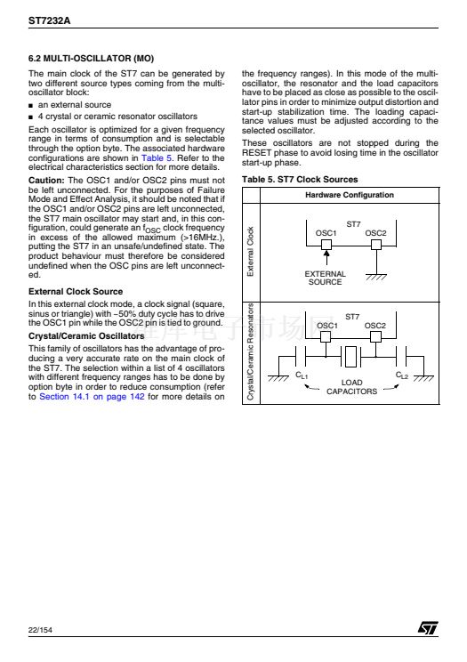
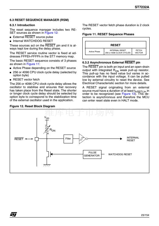
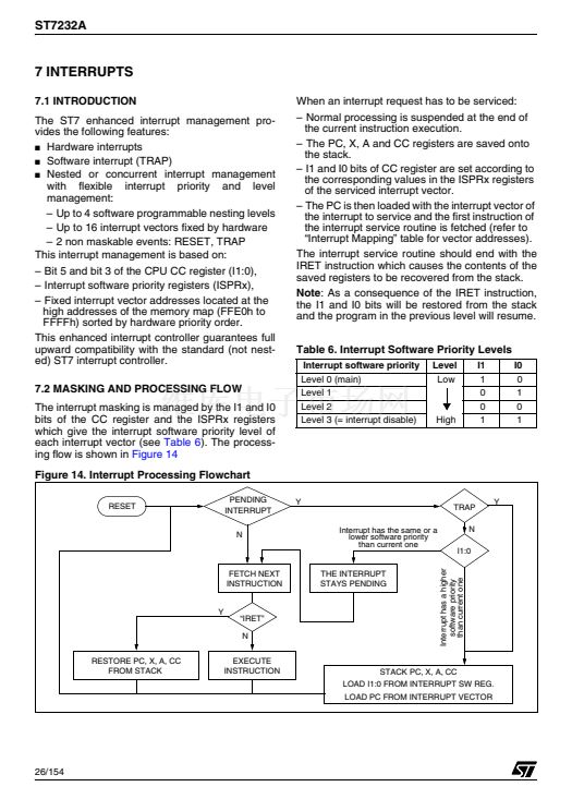
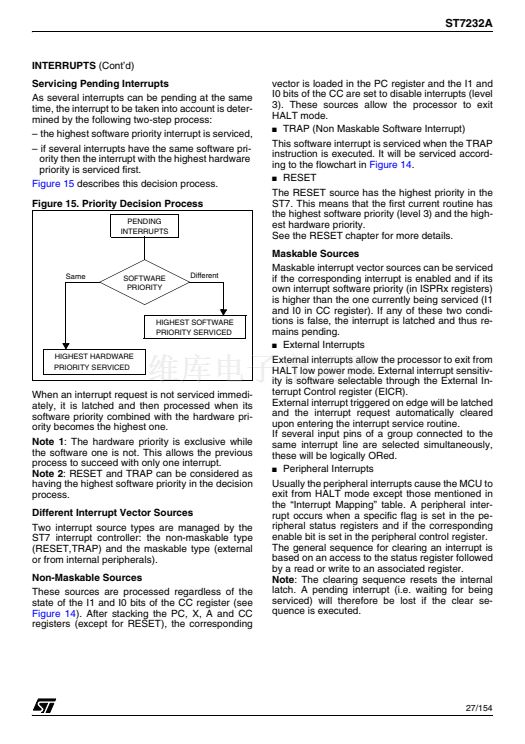
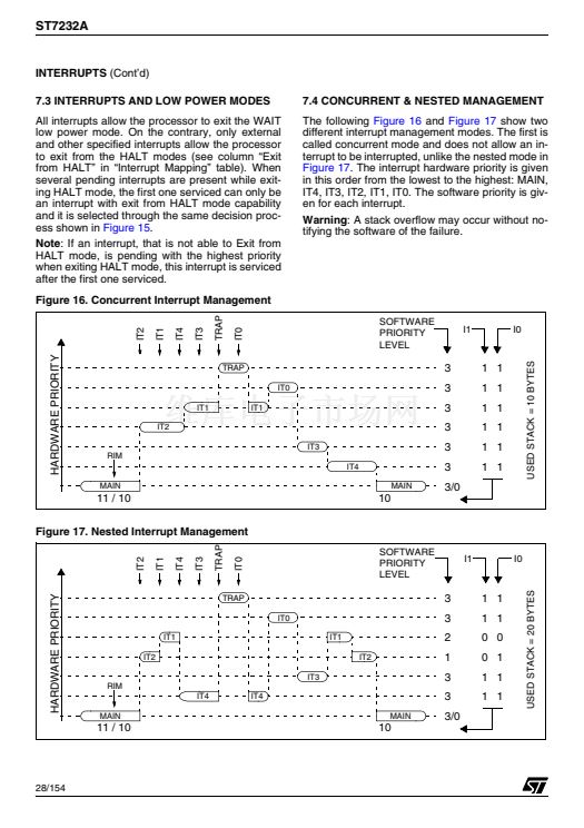
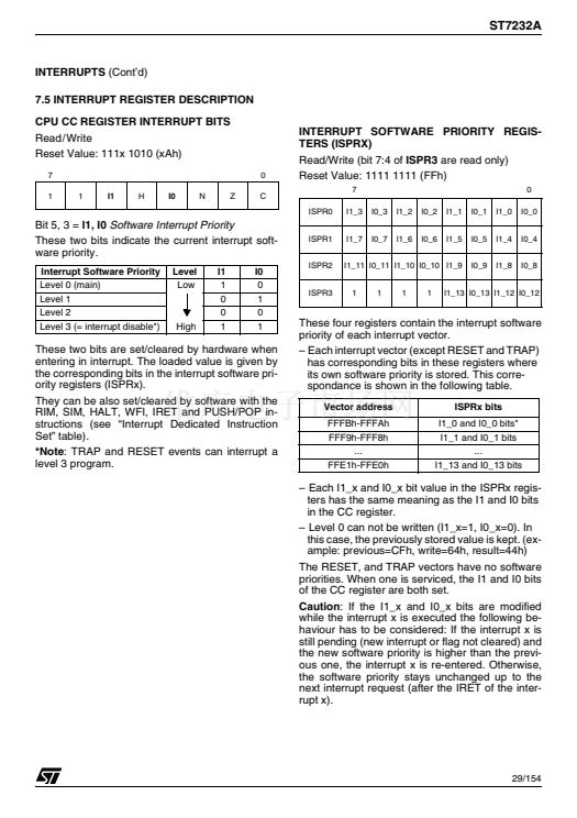
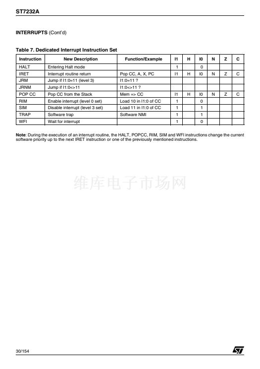
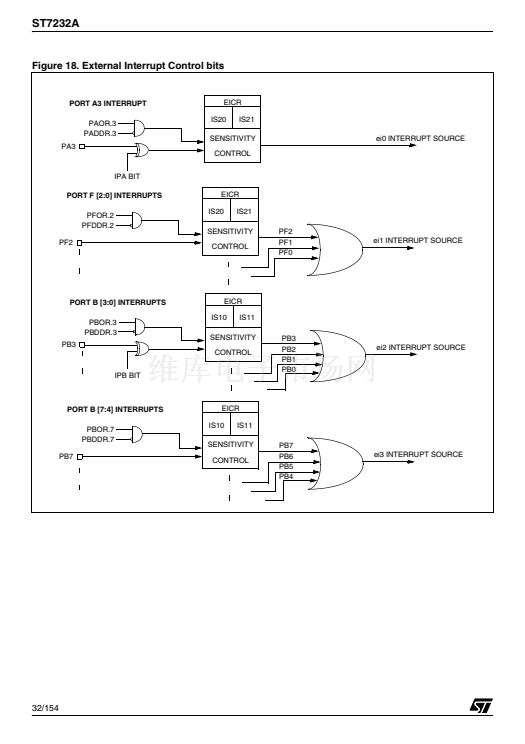
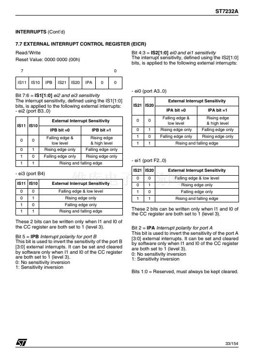
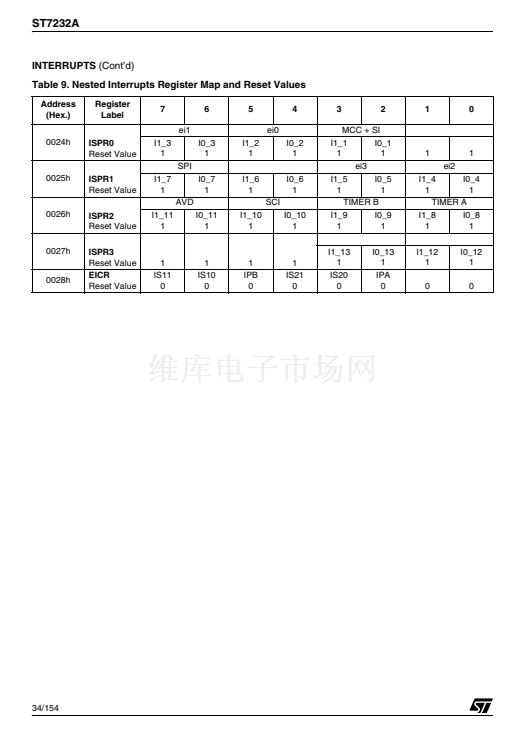
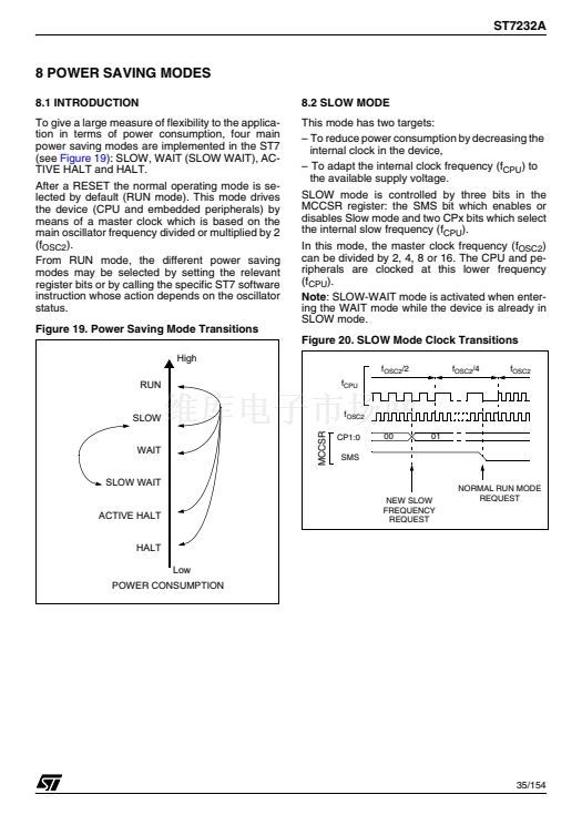
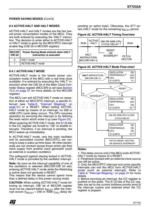
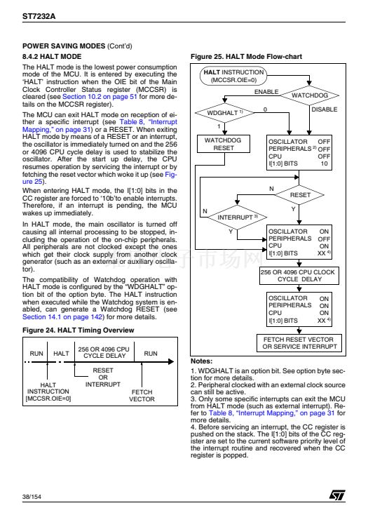
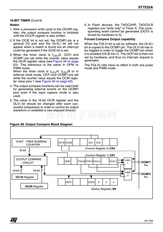
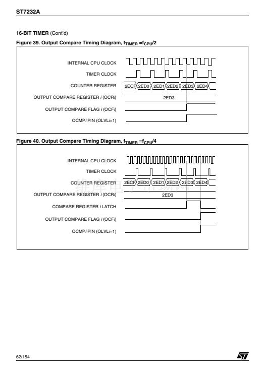
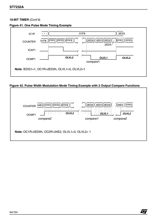
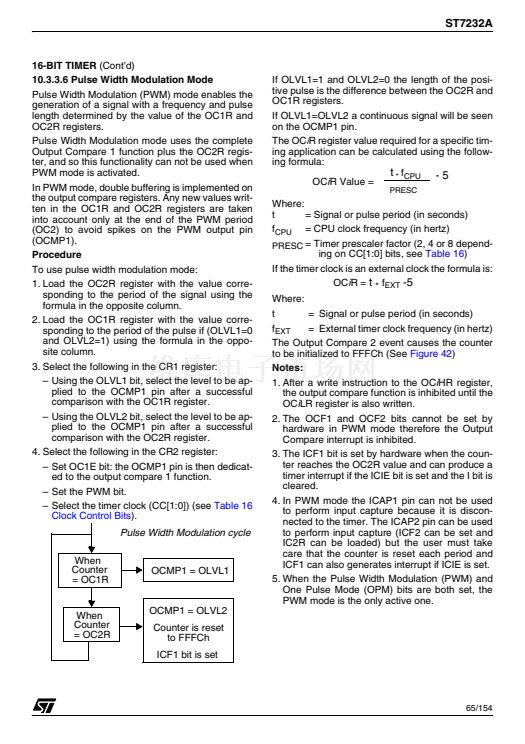
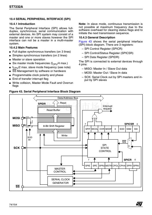
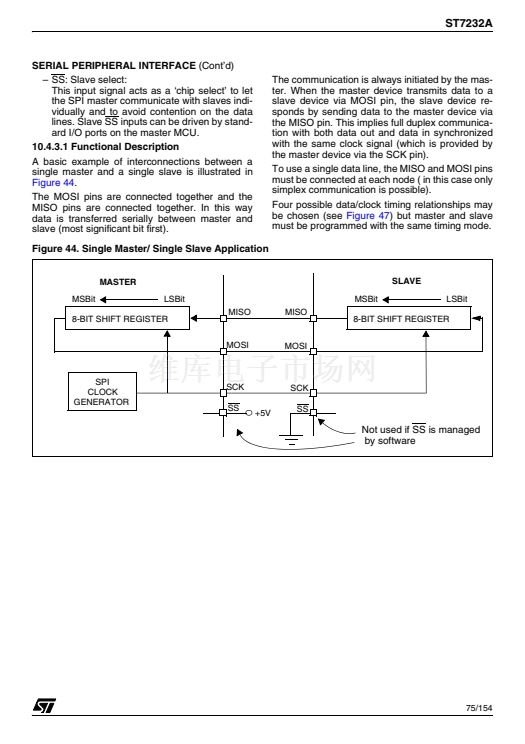
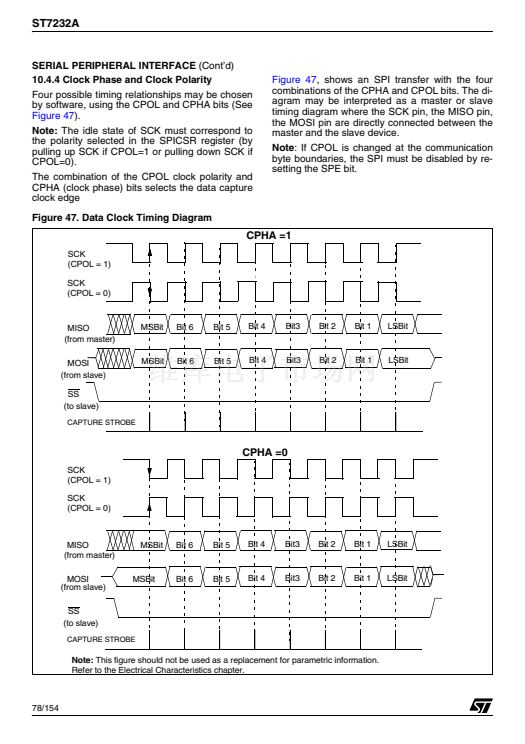
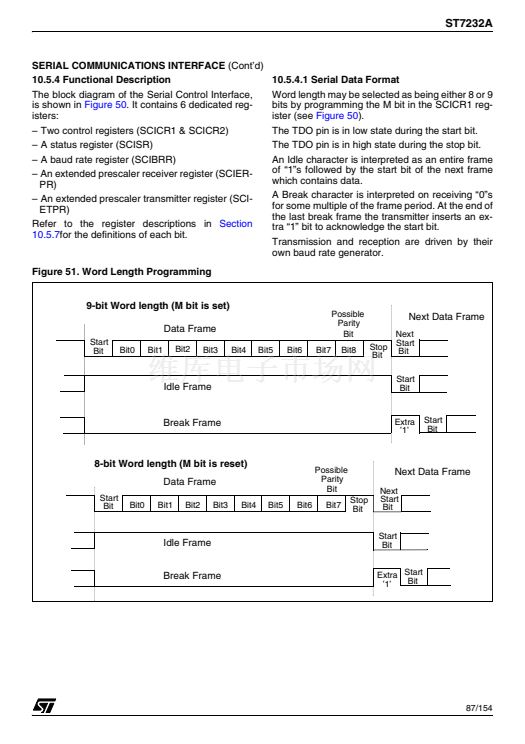
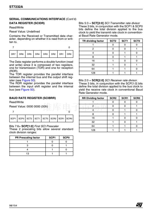
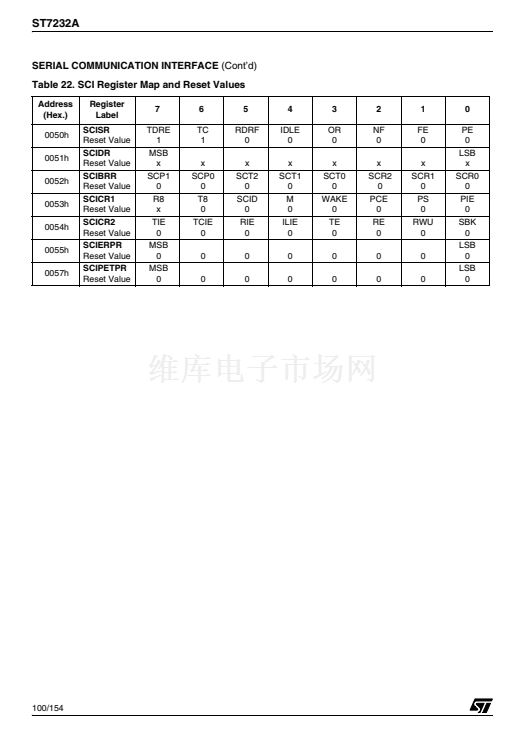
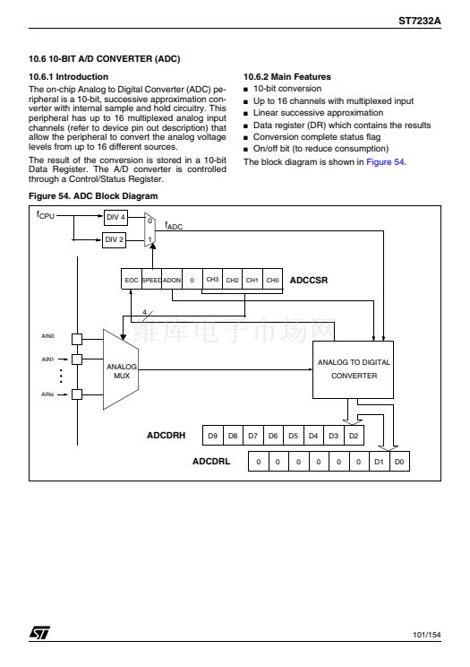
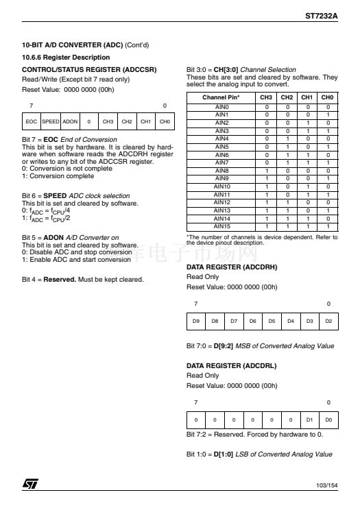
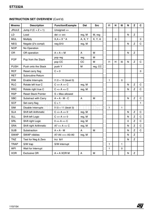
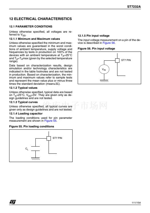
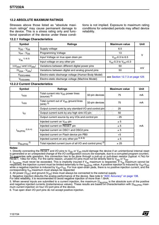
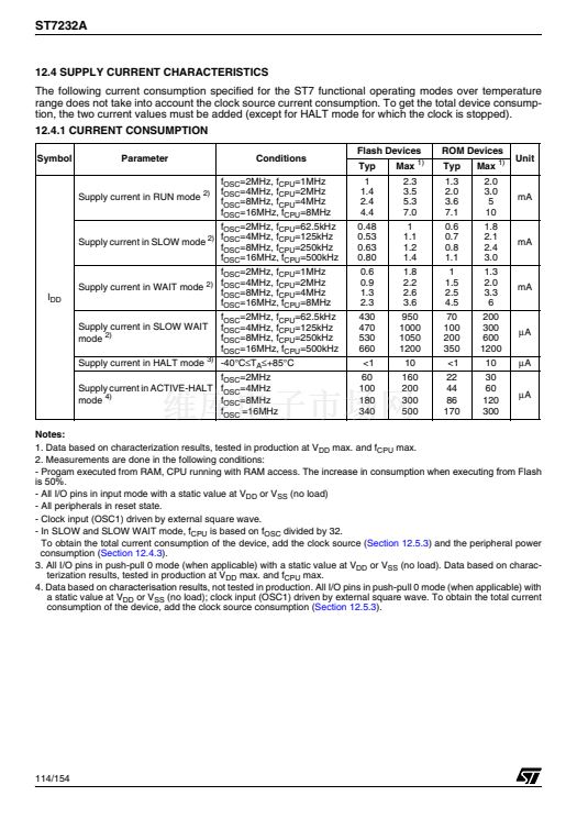
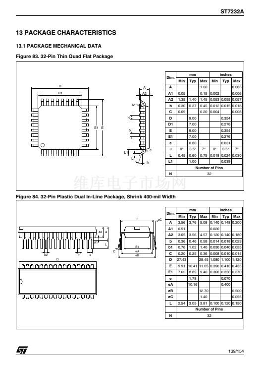
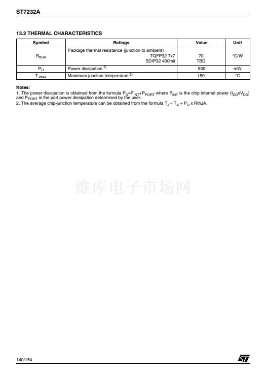
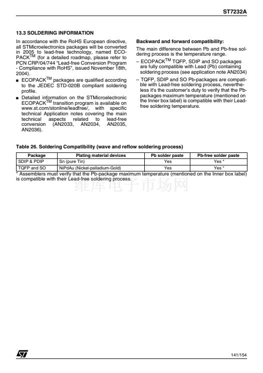
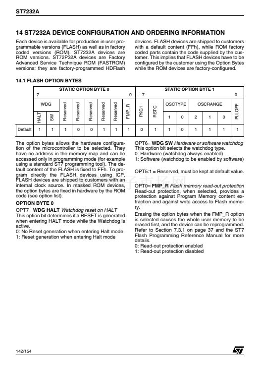
ST7232A
SERIAL COMMUNICATIONS INTERFACE
(Cont鈥檇)
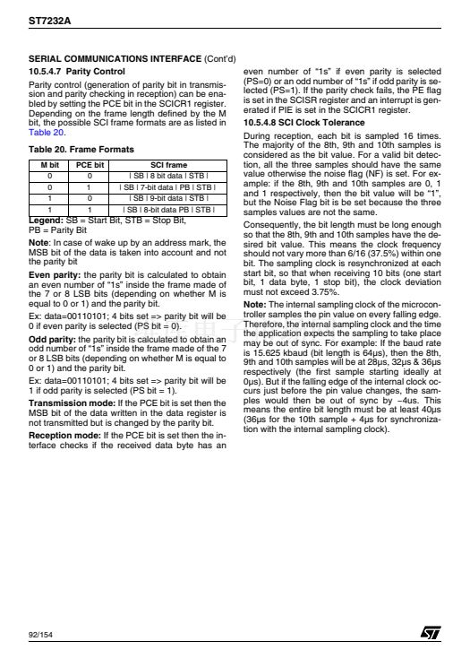
10.5.4.7 Parity Control
Parity control (generation of parity bit in transmis-
sion and parity checking in reception) can be ena-
bled by setting the PCE bit in the SCICR1 register.
Depending on the frame length defined by the M
bit, the possible SCI frame formats are as listed in
Table 20.
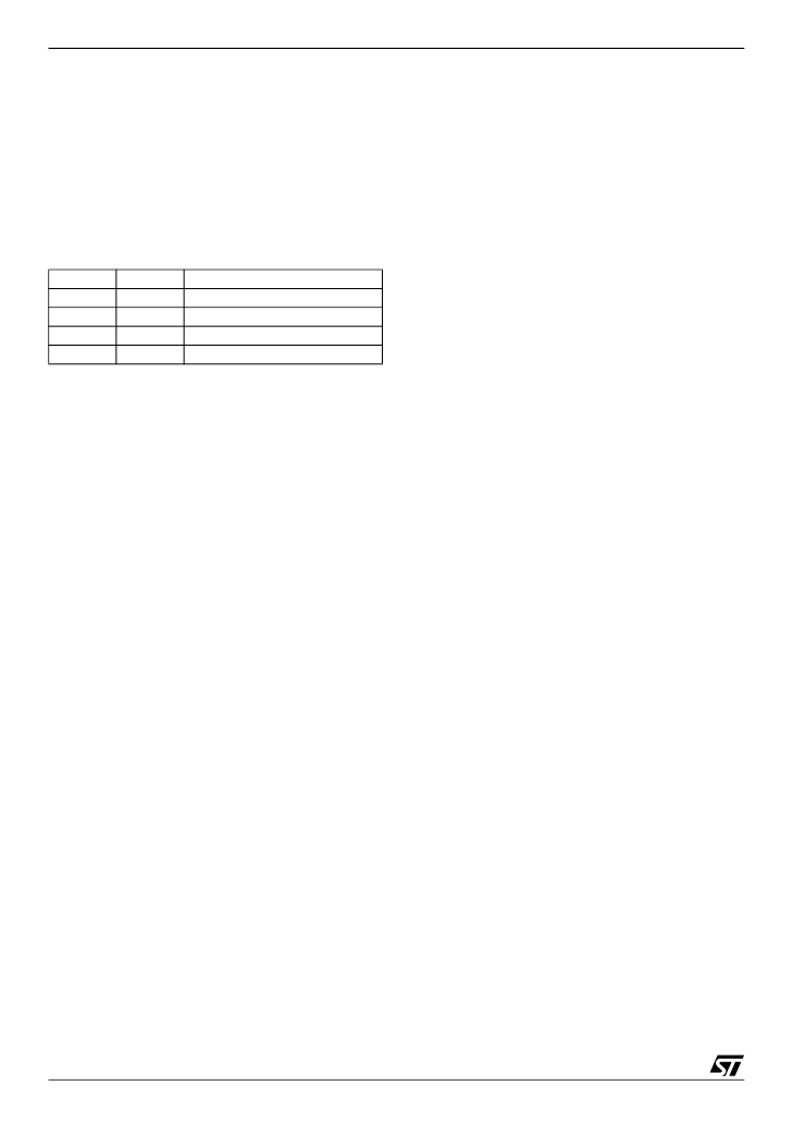
Table 20. Frame Formats
M bit
0
0
1
1
PCE bit
0
1
0
1
SCI frame
| SB | 8 bit data | STB |
| SB | 7-bit data | PB | STB |
| SB | 9-bit data | STB |
| SB | 8-bit data PB | STB |
Legend:
SB = Start Bit, STB = Stop Bit,
PB = Parity Bit
Note:
In case of wake up by an address mark, the
MSB bit of the data is taken into account and not
the parity bit
Even parity:
the parity bit is calculated to obtain
an even number of 鈥?s鈥?inside the frame made of
the 7 or 8 LSB bits (depending on whether M is
equal to 0 or 1) and the parity bit.
Ex: data=00110101; 4 bits set => parity bit will be
0 if even parity is selected (PS bit = 0).
Odd parity:
the parity bit is calculated to obtain an
odd number of 鈥?s鈥?inside the frame made of the 7
or 8 LSB bits (depending on whether M is equal to
0 or 1) and the parity bit.
Ex: data=00110101; 4 bits set => parity bit will be
1 if odd parity is selected (PS bit = 1).
Transmission mode:
If the PCE bit is set then the
MSB bit of the data written in the data register is
not transmitted but is changed by the parity bit.
Reception mode:
If the PCE bit is set then the in-
terface checks if the received data byte has an
even number of 鈥?s鈥?if even parity is selected
(PS=0) or an odd number of 鈥?s鈥?if odd parity is se-
lected (PS=1). If the parity check fails, the PE flag
is set in the SCISR register and an interrupt is gen-
erated if PIE is set in the SCICR1 register.
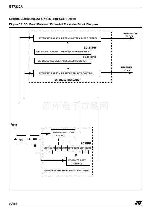
10.5.4.8 SCI Clock Tolerance
During reception, each bit is sampled 16 times.
The majority of the 8th, 9th and 10th samples is
considered as the bit value. For a valid bit detec-
tion, all the three samples should have the same
value otherwise the noise flag (NF) is set. For ex-
ample: if the 8th, 9th and 10th samples are 0, 1
and 1 respectively, then the bit value will be 鈥?鈥?
but the Noise Flag bit is be set because the three
samples values are not the same.
Consequently, the bit length must be long enough
so that the 8th, 9th and 10th samples have the de-
sired bit value. This means the clock frequency
should not vary more than 6/16 (37.5%) within one
bit. The sampling clock is resynchronized at each
start bit, so that when receiving 10 bits (one start
bit, 1 data byte, 1 stop bit), the clock deviation
must not exceed 3.75%.
Note:
The internal sampling clock of the microcon-
troller samples the pin value on every falling edge.
Therefore, the internal sampling clock and the time
the application expects the sampling to take place
may be out of sync. For example: If the baud rate
is 15.625 kbaud (bit length is 64碌s), then the 8th,
9th and 10th samples will be at 28碌s, 32碌s & 36碌s
respectively (the first sample starting ideally at
0碌s). But if the falling edge of the internal clock oc-
curs just before the pin value changes, the sam-
ples would then be out of sync by ~4us. This
means the entire bit length must be at least 40碌s
(36碌s for the 10th sample + 4碌s for synchroniza-
tion with the internal sampling clock).
92/154
1


 1
1
 2
2
 3
3
 4
4
 5
5
 6
6
 7
7
 8
8
 9
9
 10
10
 11
11
 12
12
 13
13
 14
14
 15
15
 16
16
 17
17
 18
18
 19
19
 20
20
 21
21
 22
22
 23
23
 24
24
 25
25
 26
26
 27
27
 28
28
 29
29
 30
30
 31
31
 32
32
 33
33
 34
34
 35
35
 36
36
 37
37
 38
38
 39
39
 40
40
 41
41
 42
42
 43
43
 44
44
 45
45
 46
46
 47
47
 48
48
 49
49
 50
50
 51
51
 52
52
 53
53
 54
54
 55
55
 56
56
 57
57
 58
58
 59
59
 60
60
 61
61
 62
62
 63
63
 64
64
 65
65
 66
66
 67
67
 68
68
 69
69
 70
70
 71
71
 72
72
 73
73
 74
74
 75
75
 76
76
 77
77
 78
78
 79
79
 80
80
 81
81
 82
82
 83
83
 84
84
 85
85
 86
86
 87
87
 88
88
 89
89
 90
90
 91
91
 92
92
 93
93
 94
94
 95
95
 96
96
 97
97
 98
98
 99
99
 100
100
 101
101
 102
102
 103
103
 104
104
 105
105
 106
106
 107
107
 108
108
 109
109
 110
110
 111
111
 112
112
 113
113
 114
114
 115
115
 116
116
 117
117
 118
118
 119
119
 120
120
 121
121
 122
122
 123
123
 124
124
 125
125
 126
126
 127
127
 128
128
 129
129
 130
130
 131
131
 132
132
 133
133
 134
134
 135
135
 136
136
 137
137
 138
138
 139
139
 140
140
 141
141
 142
142
 143
143
 144
144
 145
145
 146
146
 147
147
 148
148
 149
149
 150
150
 151
151
 152
152
 153
153
 154
154
