2SK1515, 2SK1516
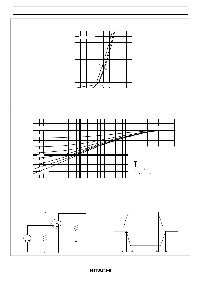
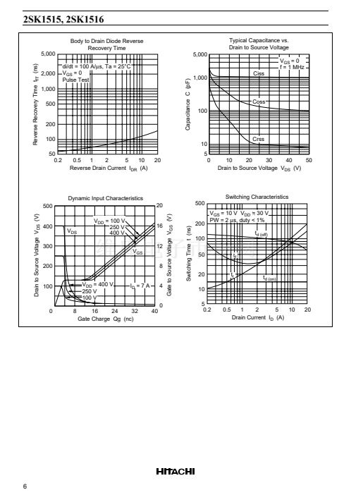
Reverse Drain Current vs.
Source to Drain Voltage
20
Reverse Drain Current I
DR
(A)
Pulse Test
16
12
15 V
8
10 V
4
V
GS
= 0, 鈥?0 V
0
0.8
2.0
0.4
1.2
1.6
Source to Drain Voltage V
SD
(V)
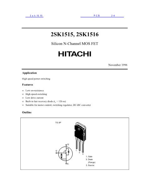
Normalized Transient Thermal Impedance
纬
S
(t)
Normalized Transient Thermal Impedance vs. Pulse Width
3
D=1
0.5
0.3
0.2
0.1
1.0
T
C
= 25掳C
0.1
0.05
0.02
胃ch鈥揷
(t) =
纬
S
(t) 路
胃ch鈥揷
胃ch鈥揷
= 1.25掳C/W, T
C
= 25掳C
P
DM
PW
D = PW
T
0.03
0.01
10
碌
0.01
Pulse
hot
1S
T
1m
10 m
100 m
Pulse Width PW (s)
100
碌
1
10
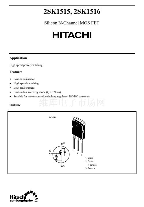
Switching Time Test Circuit
Vin Monitor
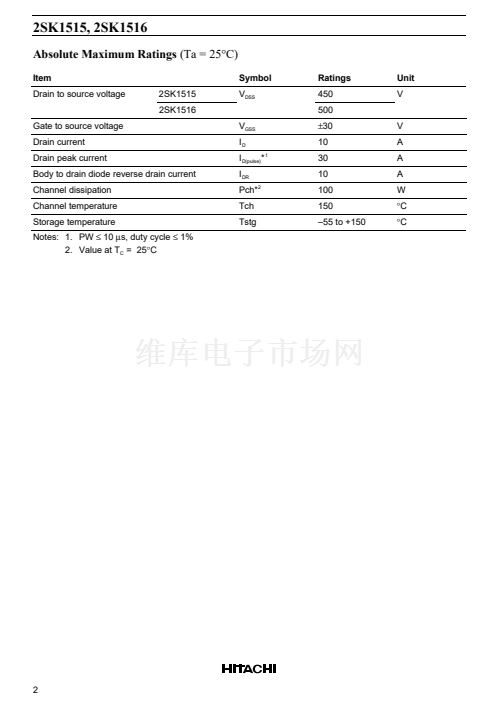
Waveforms
90%
Vout Monitor
D.U.T.
R
L
Vin
10 V
50
鈩?/div>
Vin
Vout
V
DD
.
= 30 V
.
t
d (on)
10%
10%
10%
90%
t
d (off)
t
f
90%
t
r
7


 1
1
 2
2
 3
3
 4
4
 5
5
 6
6
 7
7
 8
8
 9
9
