P
RELIMINARY
3.3V 16-Bit Transparent D-Type
T
ABLE
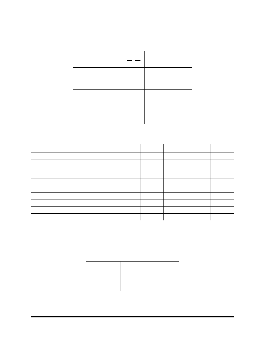
1. P
INOUT
D
ESCRIPTION
P
IN
1, 24
2, 3, 5, 6, 8, 9, 11, 12
4, 10, 15, 21, 28, 34, 39, 45
7, 31, 42
13, 14, 16, 17, 19, 20, 22, 23
25, 48
26, 27, 29, 30, 32, 31, 32,
33, 35, 36
37, 38, 40, 41, 43, 44, 46, 47
S
YMBOL
1OE-2OE
1Q1-1Q8
GND
V
CC
2Q1-2Q8
2LE-1LE
2D8-2D1
1D8-1D1
Outputs
Ground
Power Supply
Outputs
Latch Enable
Inputs
Inputs
54LVTH162373
D
ESCRIPTION
Output Enable
T
ABLE
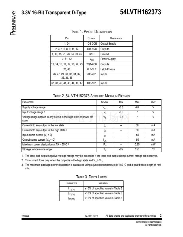
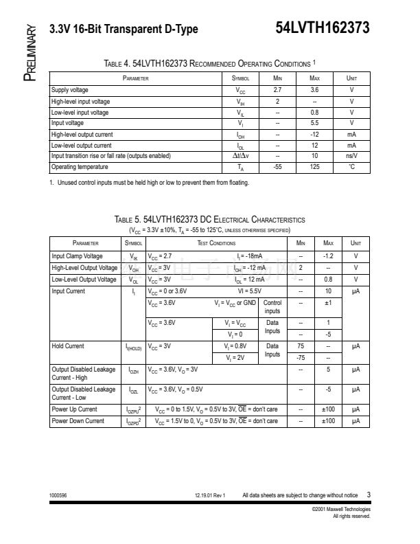
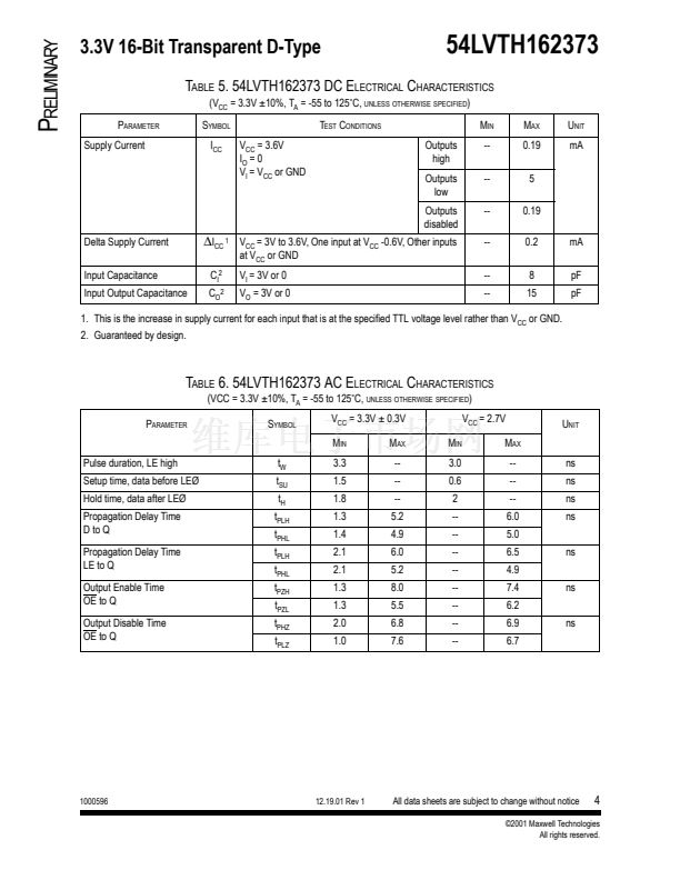
2. 54LVTH162373 A
BSOLUTE
M
AXIMUM
R
ATINGS
P
ARAMETER
Supply voltage range
Input voltage range
1
Voltage range applied to any output in the high state or power-off
state
1
Current into any output in the low state
Current into any output in the high state
2
Input clamp current (V
I
< 0)
Output clamp current (V
O
< O)
Maximum power dissipation at TA = 55
掳
C
3
Storage temperature range
S
YMBOL
V
CC
V
I
V
O
I
O
I
O
I
IK
I
OK
P
D
T
S
M
IN
-0.5
-0.5
-0.5
--
--
--
--
--
-65
M
AX
4.6
7
7
30
30
-50
-50
0.85
150
U
NIT
V
V
V
mA
mA
mA
mA
mW
掳
C
Memory
1. The input and output negative-voltage ratings may be exceeded if the input and output clamp-current ratings are observed.
2. This current flows only when the output is in the high state and V
O
> V
CC
.
3. The maximum package power dissipation is calculated using a junction temperature of 150
掳
C and a board trace length of 750
mils.
T
ABLE
3. D
ELTA
L
IMITS
P
ARAMETER
I
CC(OL)
I
CC(OH)
I
CC(OD)
V
ARIATION
卤10% of specified value in Table 5
卤10% of specified value in Table 5
卤10% of specified value in Table 5
1000596
12.19.01 Rev 1
All data sheets are subject to change without notice
2
漏2001 Maxwell Technologies
All rights reserved.


 1
1
 2
2
 3
3
 4
4
 5
5
 6
6
 7
7
 8
8
 9
9
 10
10
