Philips Semiconductors
Product specification
Quad 2-input NAND buffer (open collector)
74F38
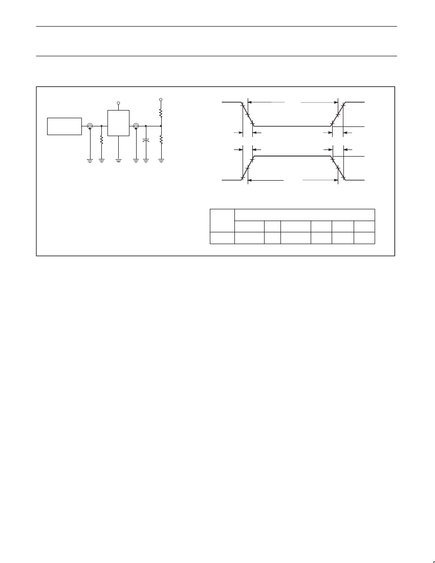
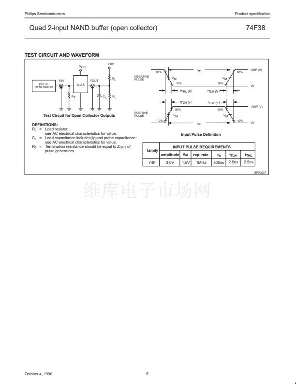
TEST CIRCUIT AND WAVEFORM
V
CC
7.0V
90%
V
IN
PULSE
GENERATOR
R
T
D.U.T.
V
OUT
R
L
NEGATIVE
PULSE
V
M
10%
t
THL (
t
f
)
C
L
R
L
t
TLH (
t
r
)
90%
POSITIVE
PULSE
10%
t
THL (
t
f
)
AMP (V)
90%
V
M
t
w
10%
0V
t
w
V
M
10%
t
TLH (
t
r
)
0V
90%
AMP (V)
Test Circuit for Open Collector Outputs
V
M
DEFINITIONS:
R
L
= Load resistor;
see AC electrical characteristics for value.
C
L
= Load capacitance includes jig and probe capacitance;
see AC electrical characteristics for value.
R
T
= Termination resistance should be equal to Z
OUT
of
pulse generators.
Input Pulse Definition
INPUT PULSE REQUIREMENTS
family
amplitude V
M
74F
3.0V
1.5V
rep. rate
1MHz
t
w
500ns
t
TLH
2.5ns
t
THL
2.5ns
SF00027
October 4, 1990
5


 1
1
 2
2
 3
3
 4
4
 5
5
 6
6
 7
7
 8
8
