鈮?/div>
4.5 V;
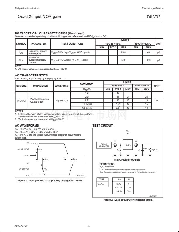
V
OL
and V
OH
are the typical output voltage drop that occur with the
output load.
V
I
nA, nB, INPUT
V
M
TEST CIRCUIT
V
cc
V
l
PULSE
GENERATOR
R
T
D.U.T.
V
O
50pF
C
L
R
L
= 1k
GND
t
PHL
V
OH
nY OUTPUT
V
M
t
PLH
Test Circuit for Outputs
DEFINITIONS
R
L
= Load resistor
C
L
= Load capacitance includes jig and probe capacitiance
R
T
= Termination resistance should be equal to Z
OUT
of pulse generators.
V
OL
SV00392
TEST
t
PLH/
t
PHL
V
CC
< 2.7V
2.7鈥?.6V
鈮?/div>
4.5 V
V
I
V
CC
2.7V
V
CC
Figure 1. Input (nA, nB) to output (nY) propagation delays.
SV00902
Figure 2. Load circuitry for switching times.
1998 Apr 20
5


 1
1
 2
2
 3
3
 4
4
 5
5
 6
6
 7
7
 8
8
 9
9
 10
10
