74LV365 Datasheet

  • 74LV365

  • Hex buffer/line driver (3-State)

  • 123.50KB

  • Philips

扫码查看芯片数据手册

上传产品规格书

PDF预览

Philips Semiconductors
Product specification
Hex buffer/line driver (3-State)
74LV365
RECOMMENDED OPERATING CONDITIONS
SYMBOL
V
CC
V
I
V
O
T
amb
DC supply voltage
Input voltage
Output voltage
Operating ambient temperature range in free air
See DC and AC
characteristics
V
CC
= 1.0V to 2.0V
V
CC
= 2.0V to 2.7V
V
CC
= 2.7V to 3.6V
PARAMETER
CONDITIONS
See Note 1
MIN
1.0
0
0
鈥?0
鈥?0
鈥?/div>
鈥?/div>
鈥?/div>
鈥?/div>
鈥?/div>
鈥?/div>
鈥?/div>
TYP
3.3
鈥?/div>
鈥?/div>
MAX
3.6
V
CC
V
CC
+85
+125
500
200
100
UNIT
V
V
V
掳C
t
r
, t
f
Input rise and fall times
ns/V
NOTE:
1. The LV is guaranteed to function down to V
CC
= 1.0V (input levels GND or V
CC
); DC characteristics are guaranteed from V
CC
= 1.2V to V
CC
= 3.6V.
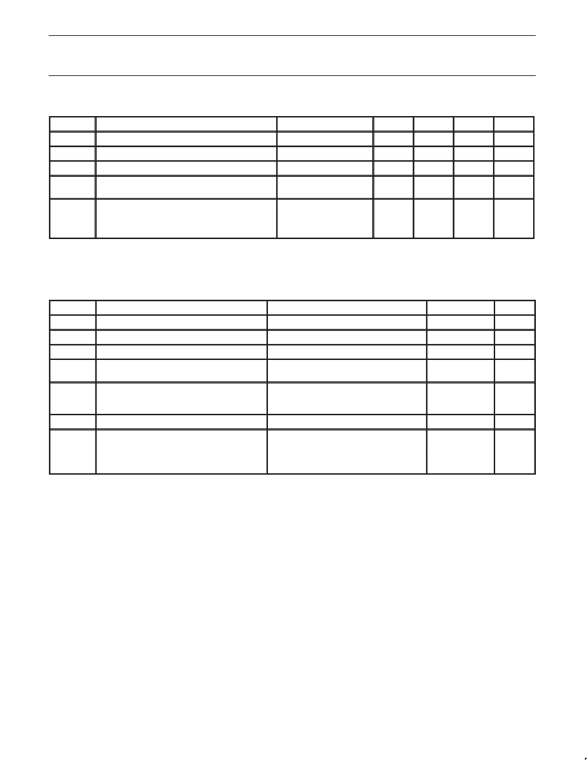
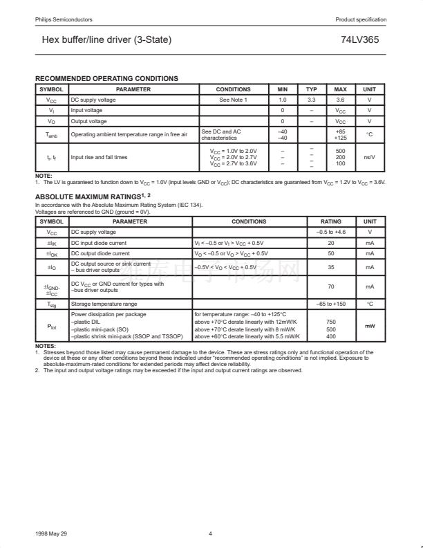
ABSOLUTE MAXIMUM RATINGS
1, 2
In accordance with the Absolute Maximum Rating System (IEC 134).
Voltages are referenced to GND (ground = 0V).
SYMBOL
V
CC
卤I
IK
卤I
OK
卤I
O
卤I
GND
,
卤I
CC
T
stg
PARAMETER
DC supply voltage
DC input diode current
DC output diode current
DC output source or sink current
鈥?bus driver outputs
DC V
CC
or GND current for types with
鈥揵us driver outputs
Storage temperature range
Power dissipation per package
鈥損lastic DIL
鈥損lastic mini-pack (SO)
鈥損lastic shrink mini-pack (SSOP and TSSOP)
for temperature range: 鈥?0 to +125掳C
above +70掳C derate linearly with 12mW/K
above +70掳C derate linearly with 8 mW/K
above +60掳C derate linearly with 5.5 mW/K
V
I
< 鈥?.5 or V
I
> V
CC
+ 0.5V
V
O
< 鈥?.5 or V
O
> V
CC
+ 0.5V
鈥?.5V < V
O
< V
CC
+ 0.5V
CONDITIONS
RATING
鈥?.5 to +4.6
20
50
35
UNIT
V
mA
mA
mA
70
鈥?5 to +150
750
500
400
mA
掳C
P
t t
tot
mW
NOTES:
1. Stresses beyond those listed may cause permanent damage to the device. These are stress ratings only and functional operation of the
device at these or any other conditions beyond those indicated under 鈥渞ecommended operating conditions鈥?is not implied. Exposure to
absolute-maximum-rated conditions for extended periods may affect device reliability.
2. The input and output voltage ratings may be exceeded if the input and output current ratings are observed.
1998 May 29
4

74LV365相关型号PDF文件下载

  • 型号
    版本
    描述
    厂商
    下载
  • 英文版
    Quad 2-input NAND gate
    PHILIPS
  • 英文版
    Quad 2-input NAND gate
    PHILIPS [P...
  • 英文版
    Quad 2-input NOR gate
    Philips
  • 英文版
    Quad 2-input NAND gate
    Philips
  • 英文版
    Hex inverter
    Philips
  • 英文版
    Quad 2-input AND gate
    Philips
  • 英文版
    Triple 3-input NAND gate
    Philips
  • 英文版
    Triple 3-input AND gate
    Philips
  • 英文版
    Hex inverting Schmitt-trigger
    Philips
  • 英文版
    Dual 4-input NAND gate
    Philips
  • 英文版
    Triple 3-input NOR gate
    Philips
  • 英文版
    Quad 2-input OR gate
    Philips
  • 英文版
    Dual D-type flip-flop with set and reset; positive-edge trig...
    PHILIPS
  • 英文版
    Dual D-type flip-flop with set and reset; positive-edge trig...
    PHILIPS [NXP Se...
  • 英文版
    Quad 2-input EXCLUSIVE-OR gate
    Philips
  • 英文版
    QUADRUPLE 2 INPUT POSITIVE NAND GATES
    TI [Texas ...
  • 英文版
    Quad 2-input NAND gate
    PHILIPS
  • 英文版
    Quad 2-input NAND gate
    PHILIPS [N...
  • 英文版
    Quad 2-input NAND gate
    PHILIPS
  • 英文版
    Quad 2-input NAND gate
    PHILIPS [N...

扫码下载APP,
一键连接广大的电子世界。

在线人工客服

买家服务:
卖家服务:

0571-85317607

客服在线时间周一至周五
9:00-17:30

关注官方微信号,
第一时间获取资讯。

建议反馈

联系人:

联系方式:

按住滑块,拖拽到最右边
>>
感谢您向阿库提出的宝贵意见,您的参与是维库提升服务的动力!意见一经采纳,将有感恩红包奉上哦!