selected. When the ORG pin is connected to Vcc, the
(x16) organization is selected. Instructions, addresses
edge of the clock (CLK). The DO pin is normally held in
ing a programming operation. The READY/BUSY
the device is ready. The DO will enter the HIGH-Z state
on the falling edge of the CS.
(DO) pins together. However, with this con铿乬uration, if
A0 is a logic-high level, it is possible for a 鈥渂us con铿俰ct鈥?/div>
to occur during the 鈥渄ummy zero鈥?that precedes the
READ operation. Under such a condition the voltage
level seen at DO is unde铿乶ed and will depend upon the
relative impedances of Data Out, and the signal source
driving A0. The higher the current sourcing capability of
A0, the higher the voltage at the DO pin.
3.3
Data Protection
3.1
START Condition
The START bit is detected by the device if CS and DI
are both high with respect to the positive edge of CLK
for the 铿乺st time.
Before a START condition is detected, CS, CLK, and DI
may change in any combination (except to that of a
START condition), without resulting in any device oper-
ation (READ, WRITE, ERASE, EWEN, EWDS, ERAL,
and WRAL). As soon as CS is high, the device is no
longer in the standby mode.
An instruction following a START condition will only be
executed if the required amount of opcodes,
addresses, and data bits for any particular instruction is
clocked in.
After execution of an instruction (i.e., clock in or out of
the last required address or data bit) CLK and DI
become don't care bits until a new START condition is
detected.
During power-up, all programming modes of operation
are inhibited until Vcc has reached a level greater than
1.4V. During power-down, the source data protection
circuitry acts to inhibit all programming modes when
Vcc has fallen below 1.4V at nominal conditions.
The ERASE/WRITE Disable (EWDS) and ERASE/
WRITE Enable (EWEN) commands give additional pro-
tection against accidentally programming during nor-
mal operation.
After power-up, the device is automatically in the
EWDS mode. Therefore, an EWEN instruction must be
performed before any ERASE or WRITE instruction can
be executed.
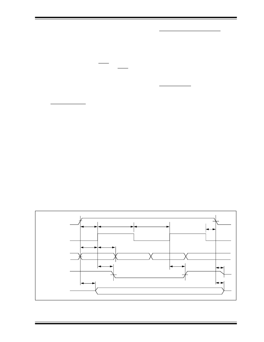
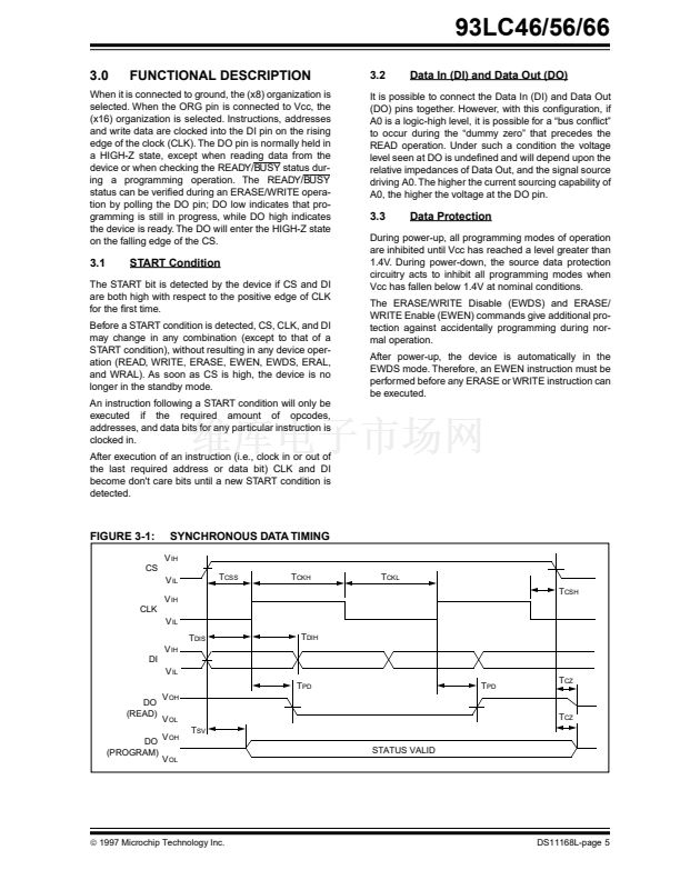
FIGURE 3-1:
CS
SYNCHRONOUS DATA TIMING
V
IH
V
IL
V
IH
T
CSS
T
CKH
T
CKL
T
CSH
CLK
V
IL
T
DIS
V
IH
DI
V
IL
T
PD
DO
(READ)
V
OH
V
OL
T
SV
STATUS VALID
T
CZ
T
PD
T
CZ
T
DIH
DO V
OH
(PROGRAM)
V
OL
漏
1997 Microchip Technology Inc.
DS11168L-page 5


 1
1
 2
2
 3
3
 4
4
 5
5
 6
6
 7
7
 8
8
 9
9
 10
10
 11
11
 12
12
