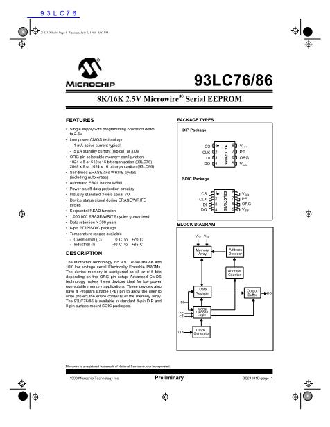
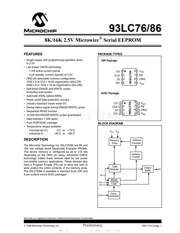
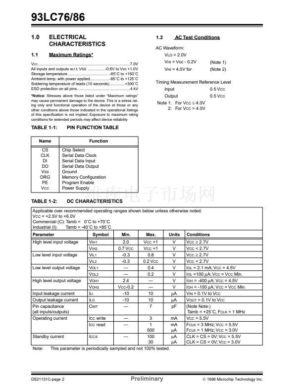
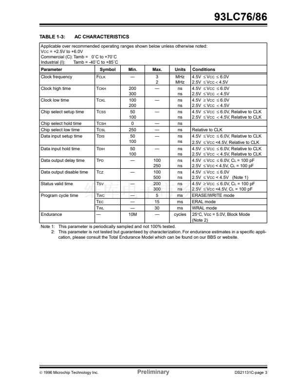
93LC76/86
3.0
3.1
DEVICE OPERATION
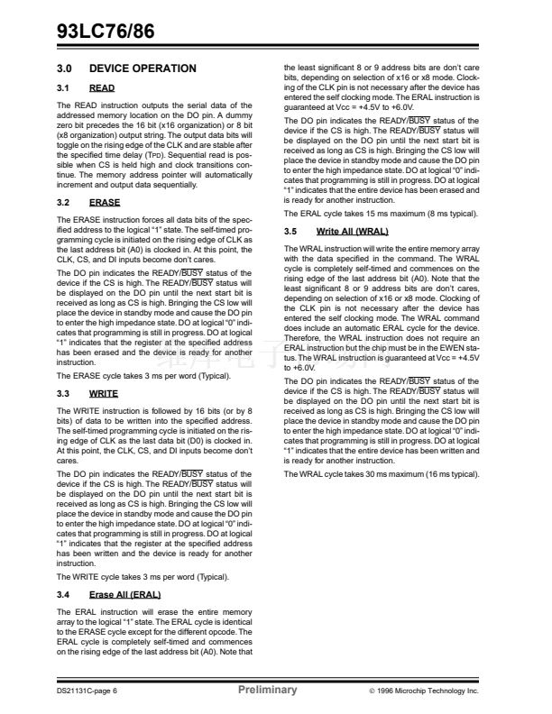
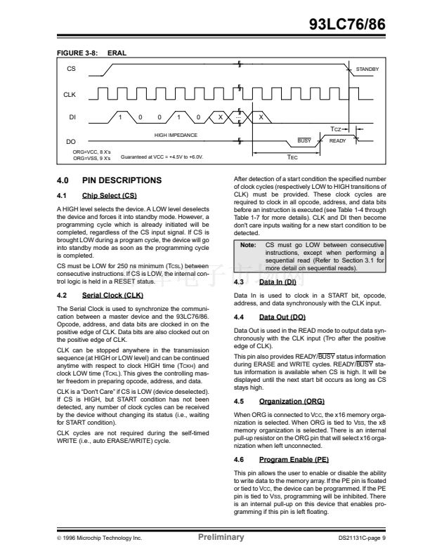
READ
The READ instruction outputs the serial data of the
addressed memory location on the DO pin. A dummy
zero bit precedes the 16 bit (x16 organization) or 8 bit
(x8 organization) output string. The output data bits will
toggle on the rising edge of the CLK and are stable after
the speci铿乪d time delay (T
PD
). Sequential read is pos-
sible when CS is held high and clock transitions con-
tinue. The memory address pointer will automatically
increment and output data sequentially.
the least signi铿乧ant 8 or 9 address bits are don鈥檛 care
bits, depending on selection of x16 or x8 mode. Clock-
ing of the CLK pin is not necessary after the device has
entered the self clocking mode. The ERAL instruction is
guaranteed at Vcc = +4.5V to +6.0V.
The DO pin indicates the READY/BUSY status of the
device if the CS is high. The READY/BUSY status will
be displayed on the DO pin until the next start bit is
received as long as CS is high. Bringing the CS low will
place the device in standby mode and cause the DO pin
to enter the high impedance state. DO at logical 鈥?鈥?indi-
cates that programming is still in progress. DO at logical
鈥?鈥?indicates that the entire device has been erased and
is ready for another instruction.
The ERAL cycle takes 15 ms maximum (8 ms typical).
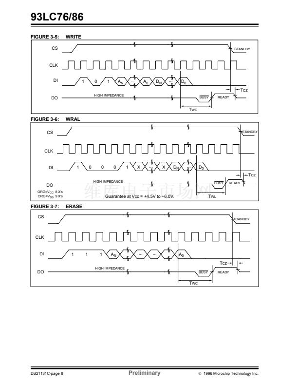
3.2
ERASE
The ERASE instruction forces all data bits of the spec-
i铿乪d address to the logical 鈥?鈥?state. The self-timed pro-
gramming cycle is initiated on the rising edge of CLK as
the last address bit (A0) is clocked in. At this point, the
CLK, CS, and DI inputs become don鈥檛 cares.
The DO pin indicates the READY/BUSY status of the
device if the CS is high. The READY/BUSY status will
be displayed on the DO pin until the next start bit is
received as long as CS is high. Bringing the CS low will
place the device in standby mode and cause the DO pin
to enter the high impedance state. DO at logical 鈥?鈥?indi-
cates that programming is still in progress. DO at logical
鈥?鈥?indicates that the register at the speci铿乪d address
has been erased and the device is ready for another
instruction.
The ERASE cycle takes 3 ms per word (Typical).
3.5
Write All (WRAL)
The WRAL instruction will write the entire memory array
with the data speci铿乪d in the command. The WRAL
cycle is completely self-timed and commences on the
rising edge of the last address bit (A0). Note that the
least signi铿乧ant 8 or 9 address bits are don鈥檛 cares,
depending on selection of x16 or x8 mode. Clocking of
the CLK pin is not necessary after the device has
entered the self clocking mode. The WRAL command
does include an automatic ERAL cycle for the device.
Therefore, the WRAL instruction does not require an
ERAL instruction but the chip must be in the EWEN sta-
tus. The WRAL instruction is guaranteed at Vcc = +4.5V
to +6.0V.
The DO pin indicates the READY/BUSY status of the
device if the CS is high. The READY/BUSY status will
be displayed on the DO pin until the next start bit is
received as long as CS is high. Bringing the CS low will
place the device in standby mode and cause the DO pin
to enter the high impedance state. DO at logical 鈥?鈥?indi-
cates that programming is still in progress. DO at logical
鈥?鈥?indicates that the entire device has been written and
is ready for another instruction.
The WRAL cycle takes 30 ms maximum (16 ms typical).
3.3
WRITE
The WRITE instruction is followed by 16 bits (or by 8
bits) of data to be written into the speci铿乪d address.
The self-timed programming cycle is initiated on the ris-
ing edge of CLK as the last data bit (D0) is clocked in.
At this point, the CLK, CS, and DI inputs become don鈥檛
cares.
The DO pin indicates the READY/BUSY status of the
device if the CS is high. The READY/BUSY status will
be displayed on the DO pin until the next start bit is
received as long as CS is high. Bringing the CS low will
place the device in standby mode and cause the DO pin
to enter the high impedance state. DO at logical 鈥?鈥?indi-
cates that programming is still in progress. DO at logical
鈥?鈥?indicates that the register at the speci铿乪d address
has been written and the device is ready for another
instruction.
The WRITE cycle takes 3 ms per word (Typical).
3.4
Erase All (ERAL)
The ERAL instruction will erase the entire memory
array to the logical 鈥?鈥?state. The ERAL cycle is identical
to the ERASE cycle except for the different opcode. The
ERAL cycle is completely self-timed and commences
on the rising edge of the last address bit (A0). Note that
DS21131C-page 6
Preliminary
漏
1996 Microchip Technology Inc.


 1
1
 2
2
 3
3
 4
4
 5
5
 6
6
 7
7
 8
8
 9
9
 10
10
 11
11
 12
12
