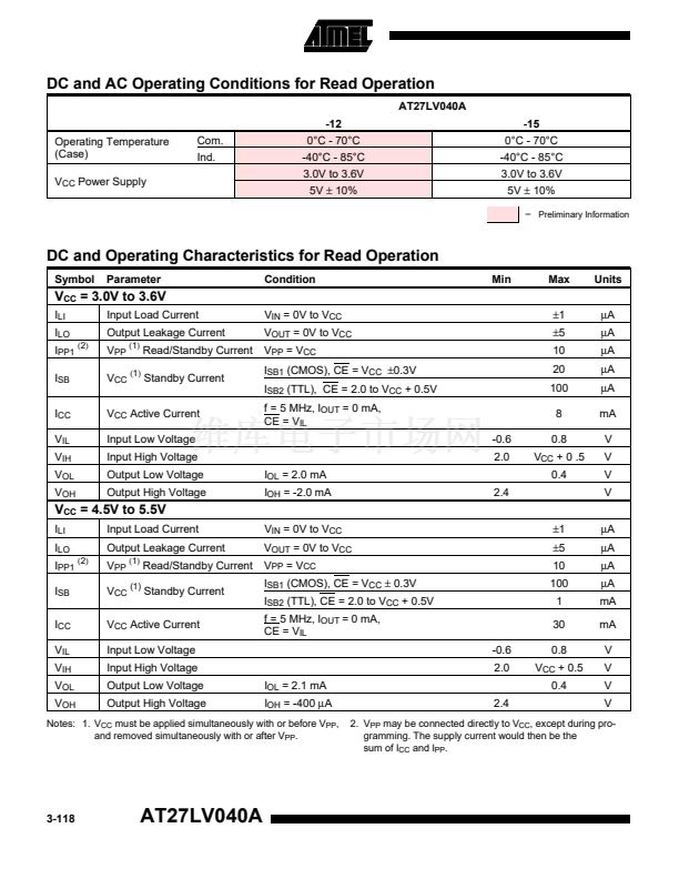
AT27LV040A
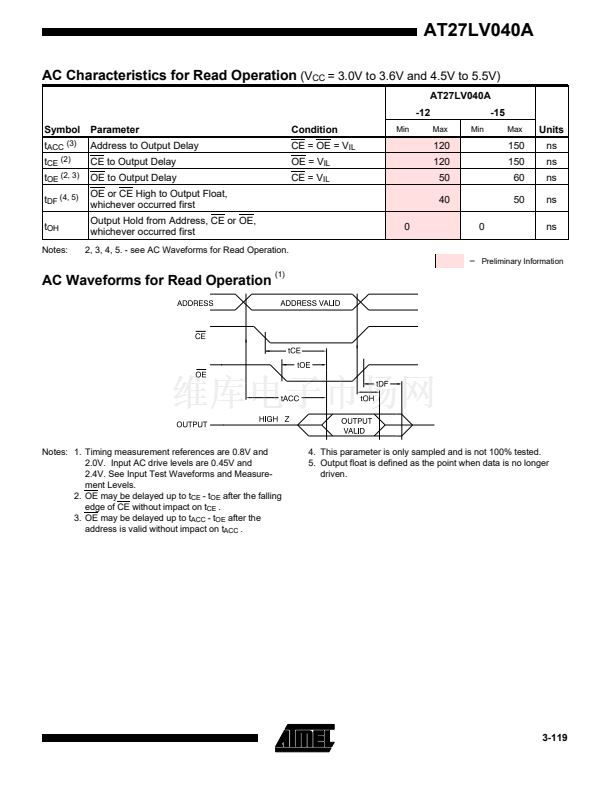
AC Characteristics for Read Operation
(V
CC
= 3.0V to 3.6V and 4.5V to 5.5V)
AT27LV040A
-12
Symbol
t
ACC (3)
t
CE (2)
t
OE (2, 3)
t
DF (4, 5)
t
OH
Notes:
-15
Max
Min
Max
Parameter
Address to Output Delay
CE to Output Delay
OE to Output Delay
OE or CE High to Output Float,
whichever occurred first
Output Hold from Address, CE or OE,
whichever occurred first
2, 3, 4, 5. - see AC Waveforms for Read Operation.
Condition
CE = OE = V
IL
OE = V
IL
CE = V
IL
Min
Units
ns
ns
ns
ns
ns
120
120
50
40
0
0
150
150
60
50
=
Preliminary Information
AC Waveforms for Read Operation
(1)
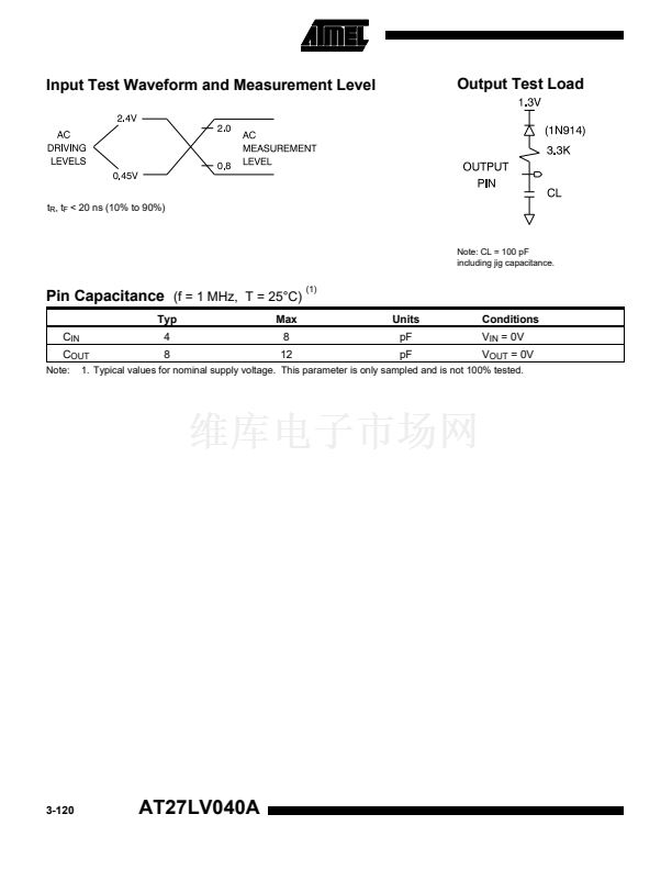
Notes: 1. Timing measurement references are 0.8V and
2.0V. Input AC drive levels are 0.45V and
2.4V. See Input Test Waveforms and Measure-
ment Levels.
2. OE may be delayed up to t
CE
- t
OE
after the falling
edge of CE without impact on t
CE
.
3. OE may be delayed up to t
ACC
- t
OE
after the
address is valid without impact on t
ACC
.
4. This parameter is only sampled and is not 100% tested.
5. Output float is defined as the point when data is no longer
driven.
3-119


 1
1
 2
2
 3
3
 4
4
 5
5
 6
6
 7
7
 8
8
 9
9
