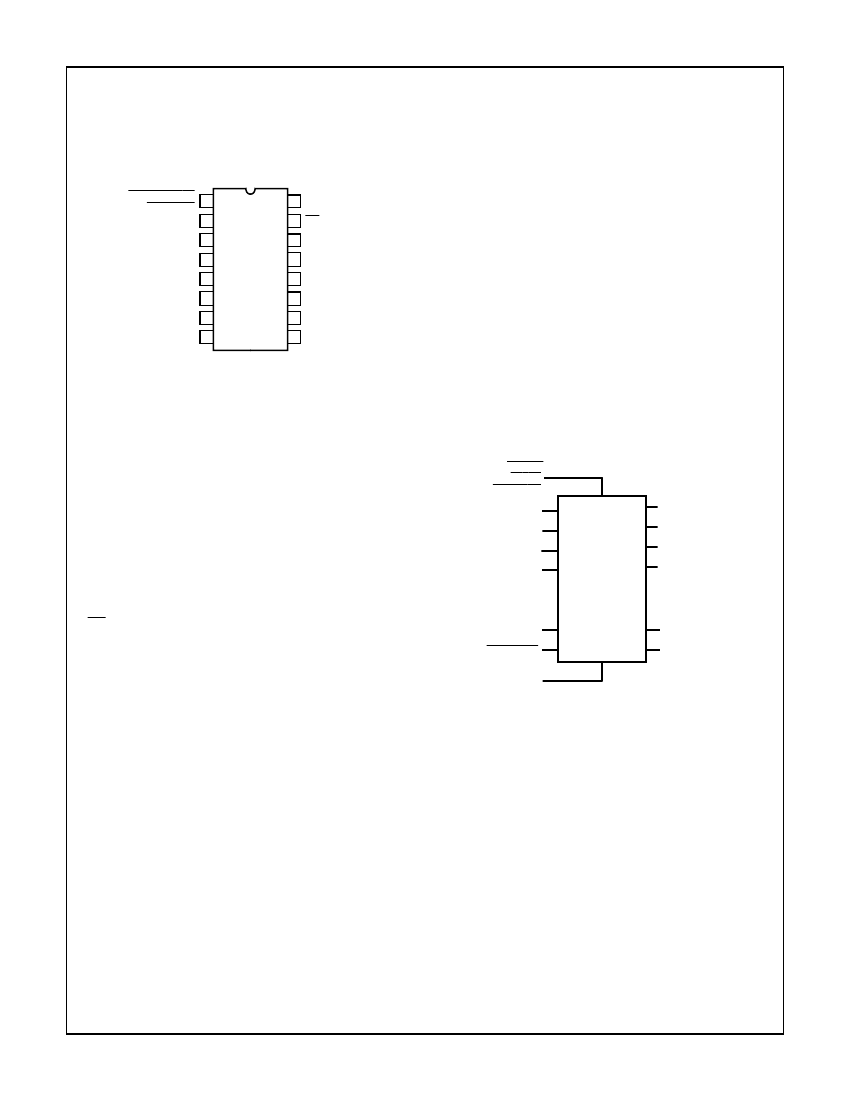
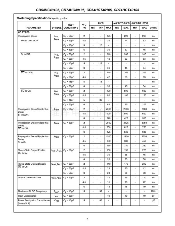
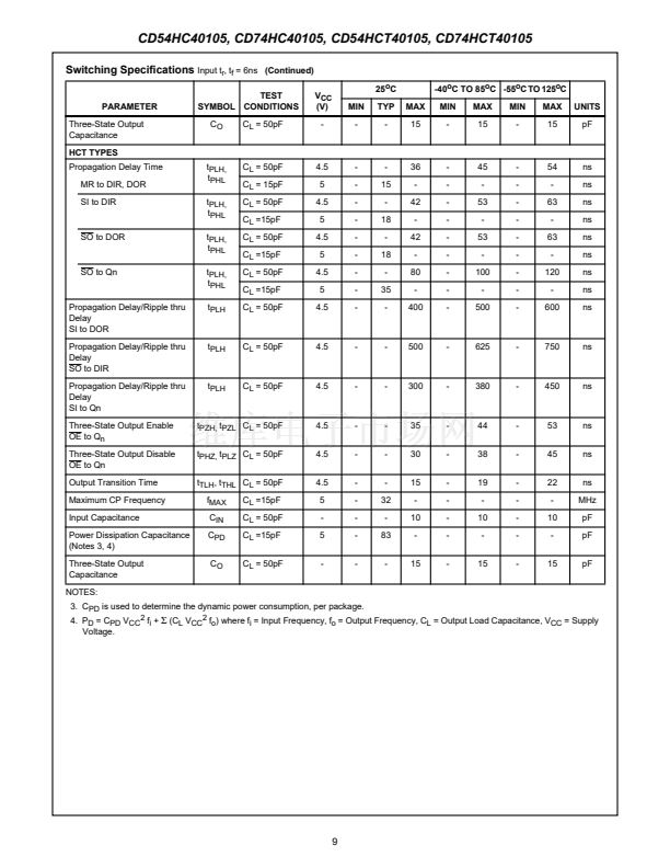
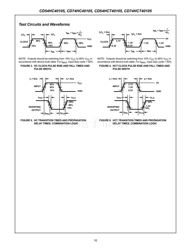
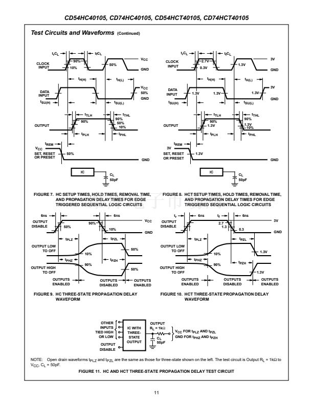
CD54HC40105, CD74HC40105, CD54HCT40105, CD74HCT40105
Pinout
CD54HC40105, CD54HCT40105
(CERDIP)
CD74HC40105, CD74HCT40105
(PDIP, SOIC)
TOP VIEW
THREE-STATE
1
CONTROL
DIR 2
SI 3
D0 4
D1 5
D2 6
D3 7
GND 8
16 V
CC
15 SO
14 DOR
13 Q0
12 Q1
11 Q2
10 Q3
9 MR
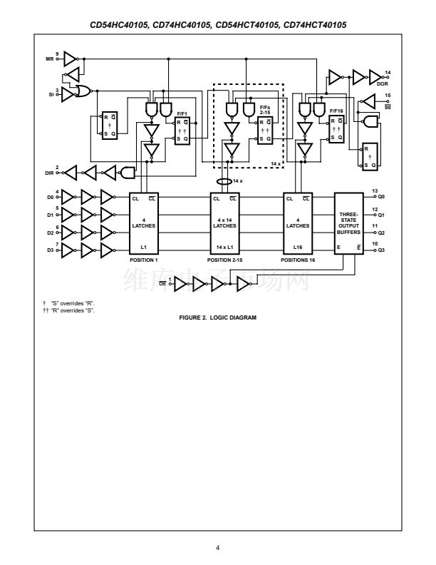
Three-State Outputs
In order to facilitate data busing, three-state outputs (Q0 to
Q3) are provided on the data output lines, while the load
condition of the register can be detected by the state of the
DOR output. A HIGH on the three-state control 铿俛g (output
enable input OE) forces the outputs into the high-impedance
OFF-state mode. Note that the shift-out signal, unlike that in
the CD40105B, is independent of the three-state output
control. In the CD40105B, the three-state control must not
be shifted from High to Low when the shift-out signal is Low
(data loss would occur). In the high-speed CMOS version
this restriction has been eliminated.
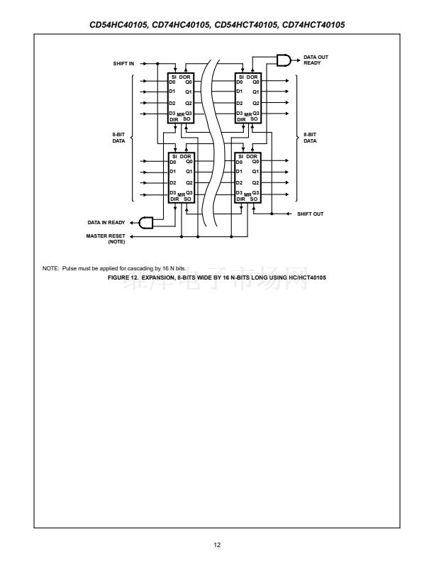
Cascading
The 40105 can be cascaded to form longer registers simply
by connecting the DIR to SO and DOR to SI. In the cascaded
mode, a MASTER RESET pulse must be applied after the
supply voltage is turned on. For words wider than four bits, the
DIR and the DOR outputs must be gated together with AND
gates. Their outputs drive the SI and SO inputs in parallel, if
expanding is done in both directions (see Figures 12 and 13).
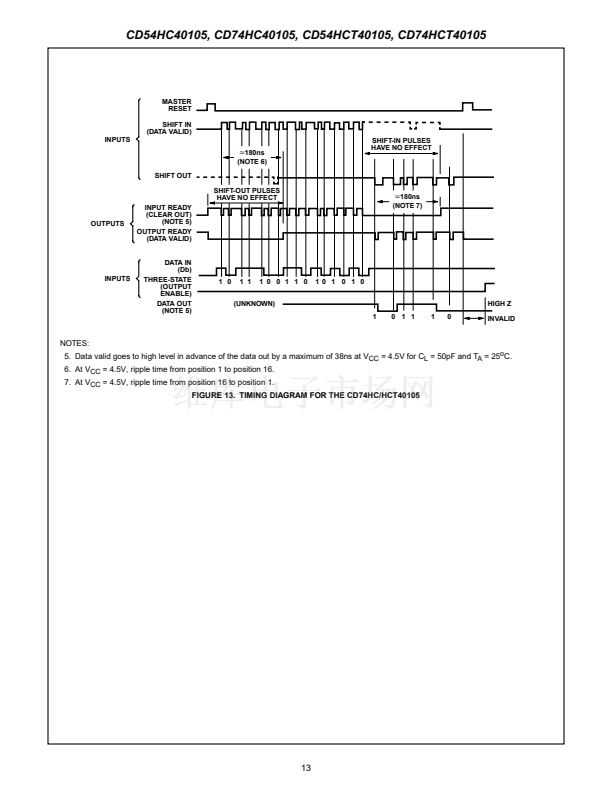
Loading Data
Data can be entered whenever the DATA-IN READY (DIR)
铿俛g is high, by a low to high transition on the SHIFT-IN (SI)
input. This input must go low momentarily before the next
word is accepted by the FIFO. The DIR 铿俛g will go low
momentarily, until the data have been transferred to the sec-
ond location. The 铿俛g will remain low when all 16-word loca-
tions are 铿乴led with valid data, and further pulses on the SI
input will be ignored until DIR goes high.
Unloading Data
As soon as the 铿乺st word has rippled to the output, the data-
out ready output (DOR) goes HIGH and data of the 铿乺st word
is available on the outputs. Data of other words can be
removed by a negative-going transition on the shift-out input
(SO). This negative-going transition causes the DOR signal
to go LOW while the next word moves to the output. As long
as valid data is available in the FIFO, the DOR signal will go
high again, signifying that the next word is ready at the
output. When the FIFO is empty, DOR will remain LOW, and
any further commands will be ignored until a 鈥?鈥?marker
ripples down to the last control register and DOR goes
HIGH. If during unloading SI is HIGH, (FIFO is full) data on
the data input of the FIFO is entered in the 铿乺st location.
Master Reset
A high on the MASTER RESET (MR) sets all the control
logic marker bits to 鈥?鈥? DOR goes low and DIR goes high.
The contents of the data register are not changed, only
declared invalid, and will be superseded when the 铿乺st word
is loaded. Thus, MR does not clear data within the register
but only the control logic. If the shift-in 铿俛g (SI) is HIGH
during the master reset pulse, data present at the input (D0
to D3) are immediately moved into the 铿乺st location upon
completion of the reset process.
Functional Diagram
THREE-
STATE
CONTROL
4
D0
5
D1
6
D2
D3
7
1
13
12
11
10
Q3
Q0
Q1
Q2
SHIFT IN
SHIFT OUT
MASTER
RESET
3
15
9
14 DATA-OUT
READY
2
DATA-IN
READY
GND = 8
V
CC
= 16
2


 1
1
 2
2
 3
3
 4
4
 5
5
 6
6
 7
7
 8
8
 9
9
 10
10
 11
11
 12
12
 13
13
 14
14
 15
15
 16
16
 17
17
 18
18
 19
19
