CED50N06/CEU50N06
V
GS
, Gate to Source Voltage (V)
15 V =48V
DS
I
D
=36A
10
3
I
D
, Drain Current (A)
12
9
6
3
0
10
2
R
DS(ON)
Limit
100ms
1ms
10ms
DC
10
1
10
0
0
10
20
30
40
10
-1
T
C
=25 C
T
J
=175 C
Single Pulse
10
-2
6
10
0
10
-1
10
1
10
2
Qg, Total Gate Charge (nC)
Figure 7. Gate Charge
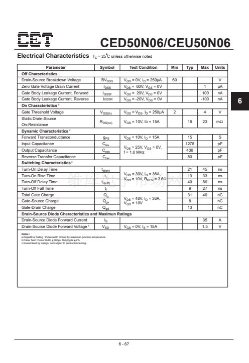
V
DD
t
on
V
IN
V
GS
R
GEN
G
R
L
D
V
OUT
t
d(on)
V
OUT
10%
V
DS
, Drain-Source Voltage (V)
Figure 8. Maximum Safe
Operating Area
t
off
t
r
90%
t
d(off)
90%
10%
t
f
INVERTED
90%
S
V
IN
50%
10%
50%
PULSE WIDTH
Figure 9. Switching Test Circuit
Figure 10. Switching Waveforms
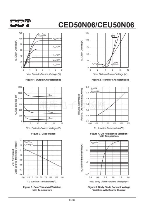
r(t),Normalized Effective
Transient Thermal Impedance
10
0
D=0.5
0.2
10
-1
0.1
0.05
0.02
0.01
Single Pulse
P
DM
t
1
t
2
10
-2
1. R
胃JC
(t)=r (t) * R
胃JC
2. R
胃JC
=See Datasheet
3. T
JM-
T
C
= P* R
胃JC
(t)
4. Duty Cycle, D=t1/t2
10
-5
10
-4
10
-3
10
-2
10
-1
10
0
10
1
Square Wave Pulse Duration (sec)
Figure 11. Normalized Thermal Transient Impedance Curve
6 - 69


 1
1
 2
2
 3
3
 4
4
