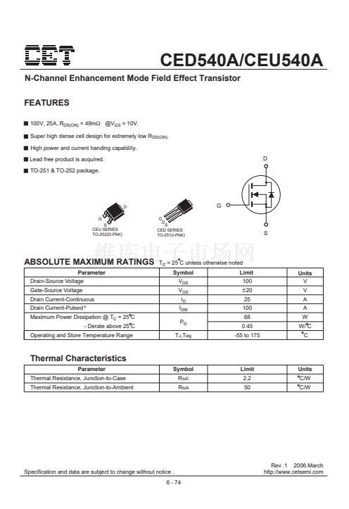
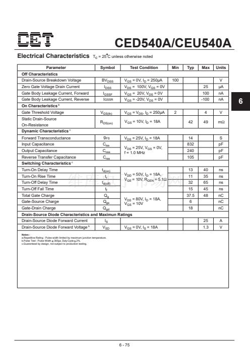
CED540A/CEU540A
80
V
GS
=10,9V
60
50
40
30
20
25 C
10
T
J
=125 C
0
0
1
2
3
4
5
6
2
4
6
8
-55 C
I
D
, Drain Current (A)
60
V
GS
=8V
40
V
GS
=7V
20
V
GS
=6V
V
GS
=5V
0
I
D
, Drain Current (A)
V
DS
, Drain-to-Source Voltage (V)
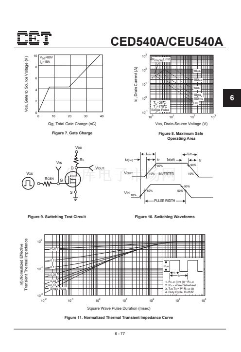
Figure 1. Output Characteristics
1200
1000
Ciss
800
600
400
Coss
200
0
0
5
10
15
20
25
Crss
3.0
2.5
2.0
1.5
1.0
0.5
0.0
-100
V
GS
, Gate-to-Source Voltage (V)
Figure 2. Transfer Characteristics
R
DS(ON),
Normalized
R
DS(ON)
, On-Resistance(Ohms)
I
D
=18A
V
GS
=10V
C, Capacitance (pF)
-50
0
50
100
150
200
V
DS
, Drain-to-Source Voltage (V)
Figure 3. Capacitance
1.3
1.2
1.1
1.0
0.9
0.8
0.7
0.6
-50
T
J
, Junction Temperature( C)
Figure 4. On-Resistance Variation
with Temperature
V
GS
=0V
2
V
TH
, Normalized
Gate-Source Threshold Voltage
V
DS
=V
GS
I
D
=250碌A
I
S
, Source-drain current (A)
25
50
75
100
125
150
10
10
1
10
-25
0
0
0.4
0.6
0.8
1.0
1.2
1.4
T
J
, Junction Temperature( C)
Figure 5. Gate Threshold Variation
with Temperature
V
SD
, Body Diode Forward Voltage (V)
Figure 6. Body Diode Forward Voltage
Variation with Source Current
6 - 76


 1
1
 2
2
 3
3
 4
4
