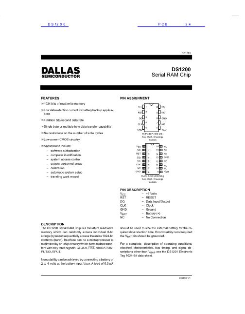
DS1200
ADDRESS/COMMAND
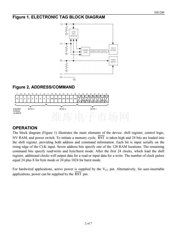
Each memory transfer consists of a 3-byte input called the address/command. The address/command is
shown in Figure 2. As defined, the first byte of the address/command specifies whether the memory is
written or read. If any one of the bits of the first byte of the address/command fail to meet the exact
pattern of read or write, the cycle is aborted and all future inputs to the tag are ignored until RST is
brought low and then high again to begin a new cycle. The 8-bit pattern for read is 10011101. The second
byte of the address/command describes address inputs A0 in bit 0 through A6 in bit 6. Bit 7 of the second
byte of the address/command word must be set to logic 0. If bit 7 does not equal logic 0, the cycle is
aborted and all future inputs to the tag are ignored until RST is brought low and then high again to begin
a new cycle. The third byte of the address/command (bits 0 through 6) must be set to logic 0 or the cycle
is aborted and all future inputs are ignored until RST is brought low and then high again to begin a new
cycle. Bit 7 of byte 3 of the address/command is used along with address bits A0 through A6 to define
burst mode. When A0 through A6 equals logic 0 and bit 7 of byte 3 of the address command equals logic
1, the tag will enter the burst mode after the address/command sequence is complete.
BURST MODE
Burst mode is when all address bits (A0 to A6) of the address/command are set to logic 0 and bit 7 of byte
3 to logic 1. The burst mode causes 128 consecutive bytes to be read or written. Burst mode terminates
when the RST input is driven low.
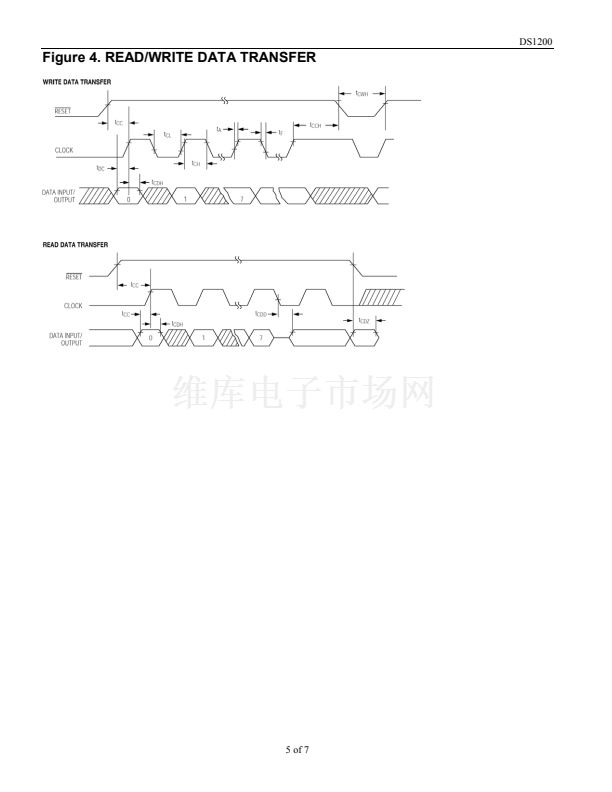
RESET AND CLOCK CONTROL
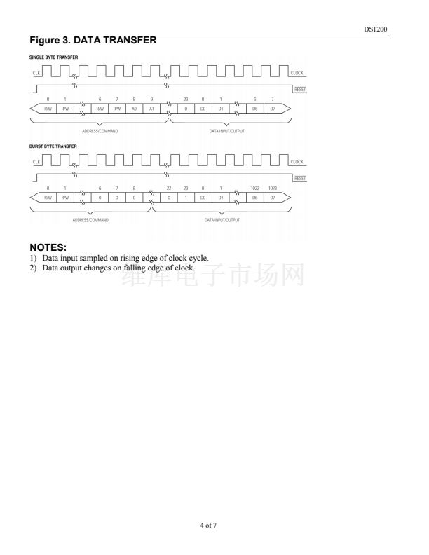
All data transfers are initiated by driving the RST input high. The RST input serves three functions.
First, RST turns on the control logic, which allows access to the shift register for the address/command
sequence. Second, the RST signal provides a power source for the cycle to follow. To meet this
requirement, a drive source for RST of 2mA at 3.8V is required. However if the V
CC
pin is connected to
a 5V source within nominal limits, then the RST pin is not used as a source of power and input levels
revert to normal V
IH
and V
IL
inputs with a drive current requirement of 500
mA
. Finally, the RST signal
provides a method of terminating either single byte or multiple byte data transfers. A clock cycle is a
sequence of falling edge followed by a rising edge. For data inputs, the data must be valid during the
rising edge of the clock cycle. Address/command bits and data bits are input on the rising edge of the
clock and data bits are output on the falling edge of the clock. All data transfer terminates if the RST
input is low and DQ pin goes to a high-impedance state. When data transfer to the serial RAM chip is
terminated using, RST , the transition of RST must occur while the clock is at high level to avoid
disturbing the last bit of data. Data transfer is illustrated in Figure 3.
DATA INPUT
Following the 24 clock cycles that input an address/command, a data byte is input on the rising edge of
the next eight clock cycles, assuming that the read/write and write/read bits are properly set (for data
input byte 1, bit 0 = 1; bit 1 = 0; bit 2 = 1; bit 3 = 1; bit 4 = 1; bit 5 = 0; bit 6 = 0; bit 7 = 1).
DATA OUTPUT
Following the 24 clock cycles that input the read mode, a data byte is output on the falling edge of the
next eight clock cycles (for data output byte 1, bit 0 = 0; bit 1 = 1; bit 2 = 0; bit 3= 0; bit 4 = 0; bit 5 = 1;
bit 6 = 1; bit 7 = 0).
3 of 7


 1
1
 2
2
 3
3
 4
4
 5
5
 6
6
 7
7
