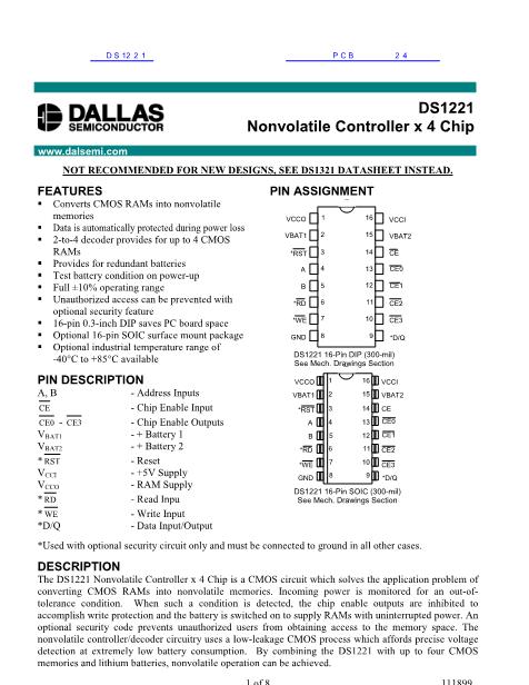
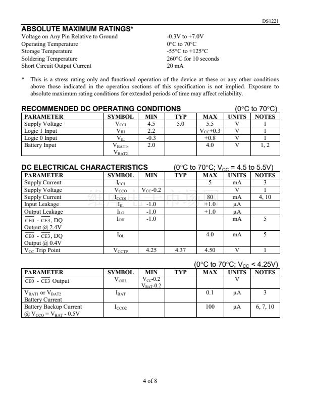
DS1221
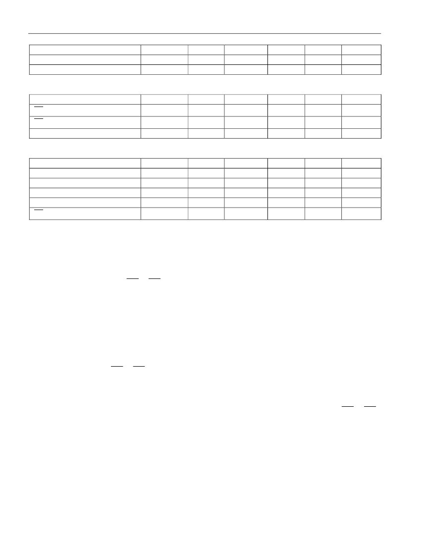
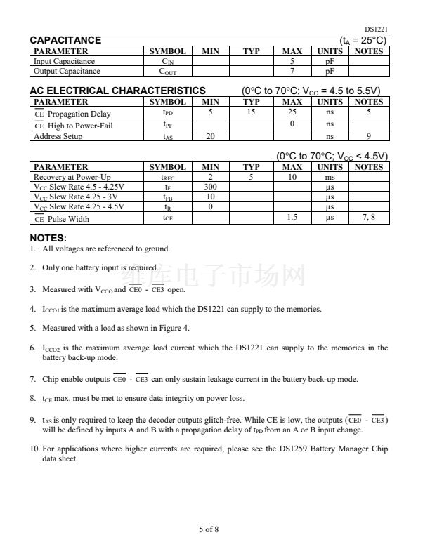
CAPACITANCE
PARAMETER
Input Capacitance
Output Capacitance
SYMBOL
C
IN
C
OUT
MIN
TYP
MAX
5
7
(t
A
= 25掳C)
UNITS
pF
pF
NOTES
AC ELECTRICAL CHARACTERISTICS
PARAMETER
CE
Propagation Delay
CE
High to Power-Fail
Address Setup
SYMBOL
t
PD
t
PF
t
AS
MIN
5
20
(0掳C to 70掳C; V
CC
= 4.5 to 5.5V)
TYP
15
MAX
25
0
UNITS
ns
ns
ns
NOTES
5
9
(0掳C to 70掳C; V
CC
< 4.5V)
PARAMETER
Recovery at Power-Up
V
CC
Slew Rate 4.5 - 4.25V
V
CC
Slew Rate 4.25 - 3V
V
CC
Slew Rate 4.25 - 4.5V
CE
Pulse Width
SYMBOL
t
REC
t
F
t
FB
t
R
t
CE
MIN
2
300
10
0
TYP
5
MAX
10
UNITS
ms
碌s
碌s
碌s
碌s
NOTES
1.5
7, 8
NOTES:
1. All voltages are referenced to ground.
2. Only one battery input is required.
3. Measured with V
CCO
and
CE0
-
CE3
open.
4. I
CCO1
is the maximum average load which the DS1221 can supply to the memories.
5. Measured with a load as shown in Figure 4.
6. I
CCO2
is the maximum average load current which the DS1221 can supply to the memories in the
battery back-up mode.
7. Chip enable outputs
CE0
-
CE3
can only sustain leakage current in the battery back-up mode.
8. t
CE
max. must be met to ensure data integrity on power loss.
9. t
AS
is only required to keep the decoder outputs glitch-free. While CE is low, the outputs (
CE0
-
CE3
)
will be defined by inputs A and B with a propagation delay of t
PD
from an A or B input change.
10. For applications where higher currents are required, please see the DS1259 Battery Manager Chip
data sheet.
5 of 8


 1
1
 2
2
 3
3
 4
4
 5
5
 6
6
 7
7
 8
8
