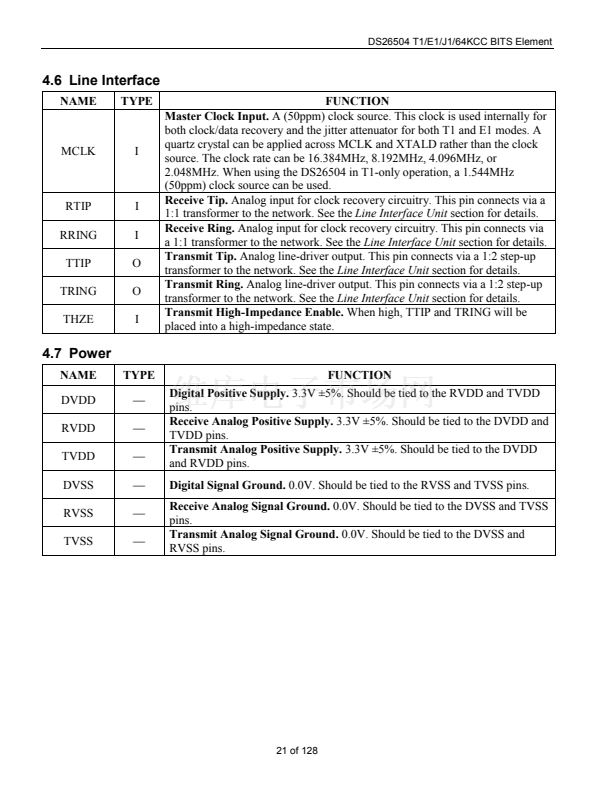
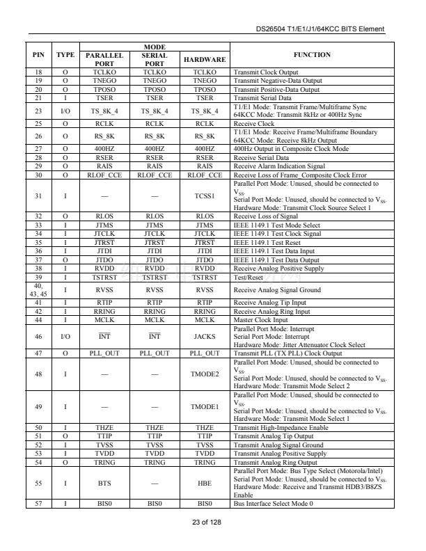
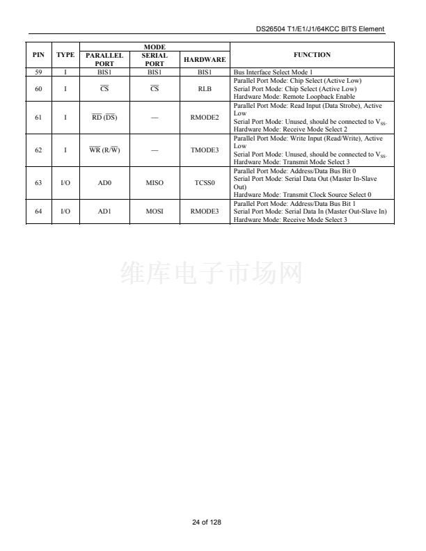
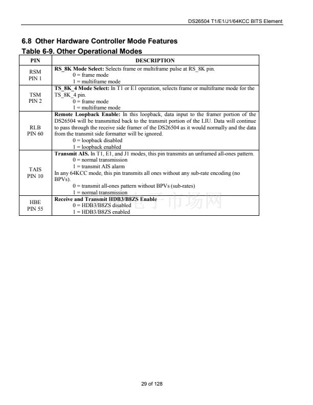
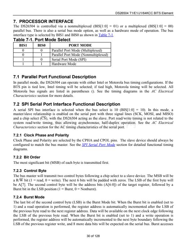
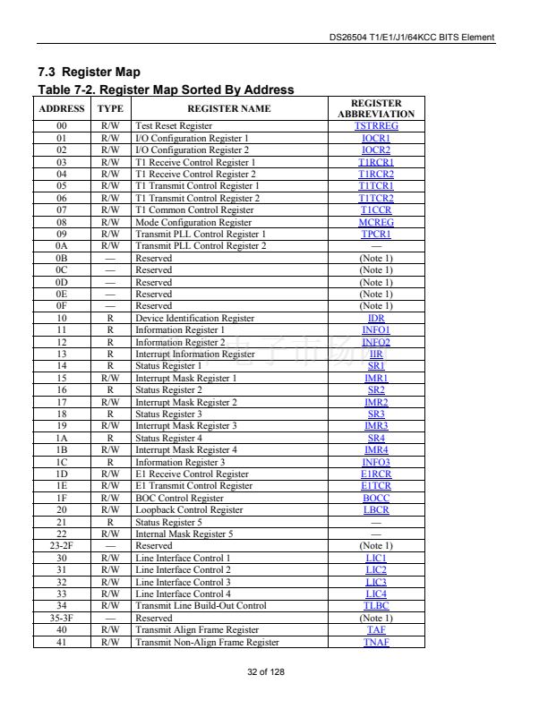
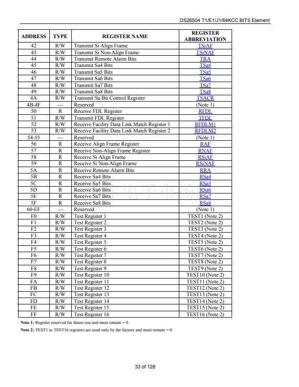
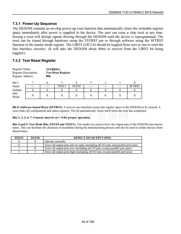
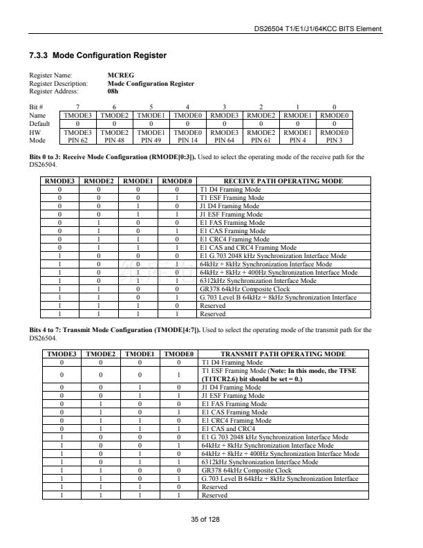
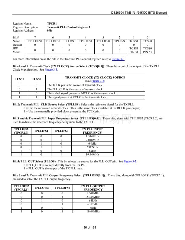
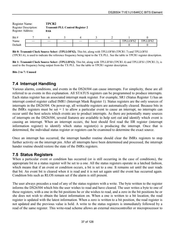
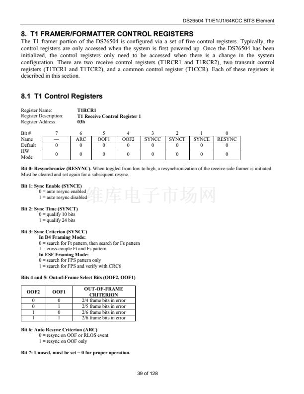
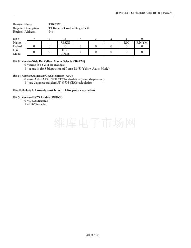
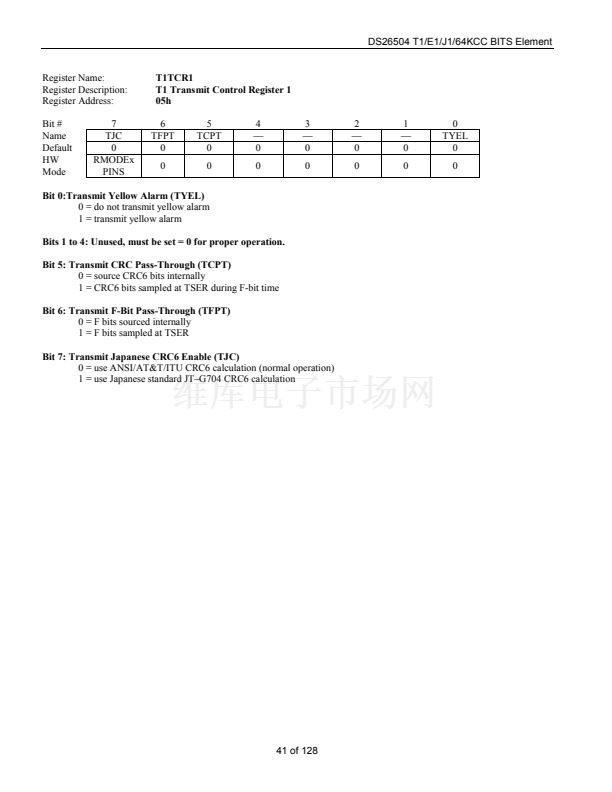
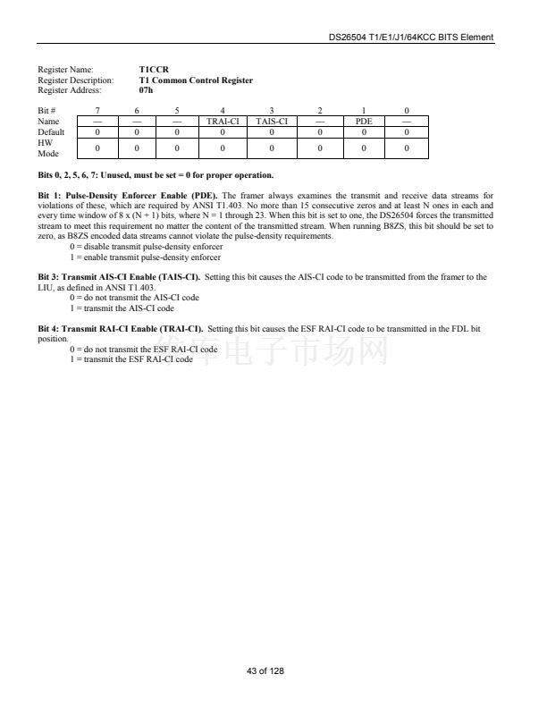
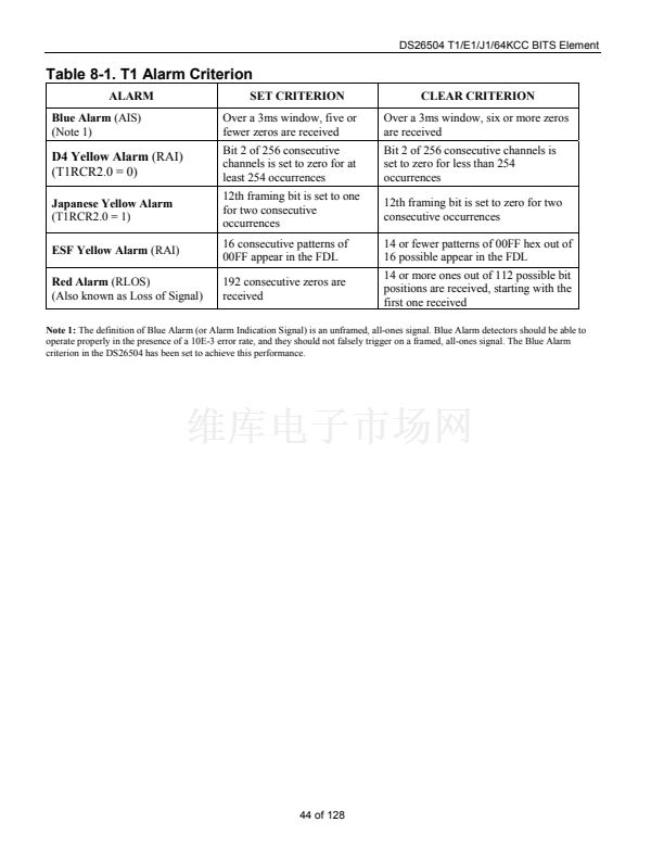
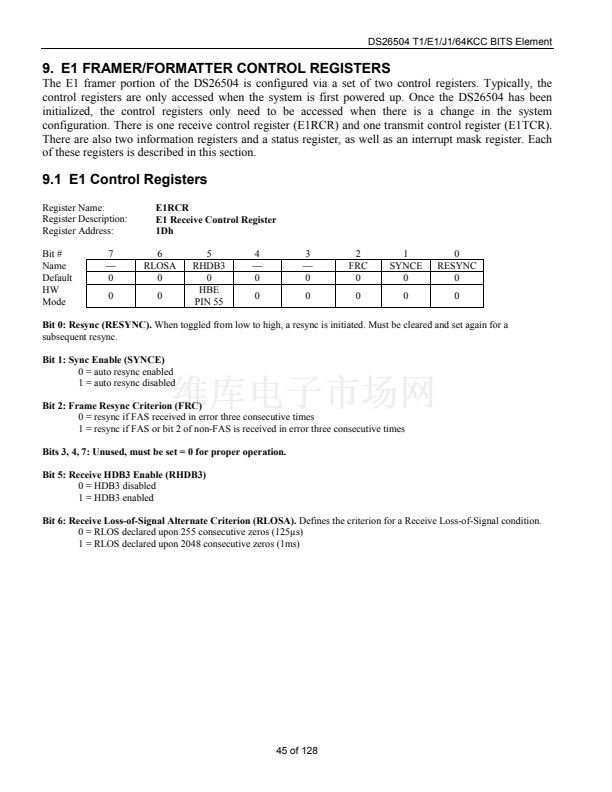
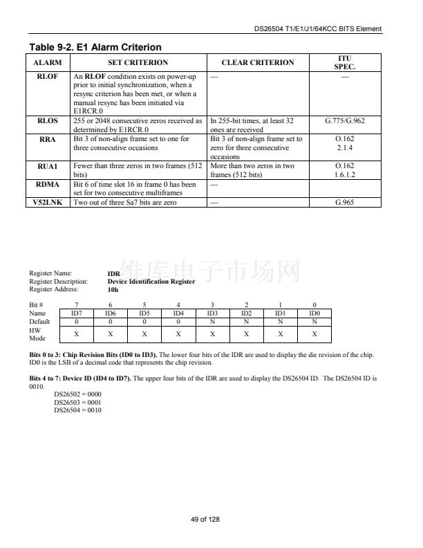
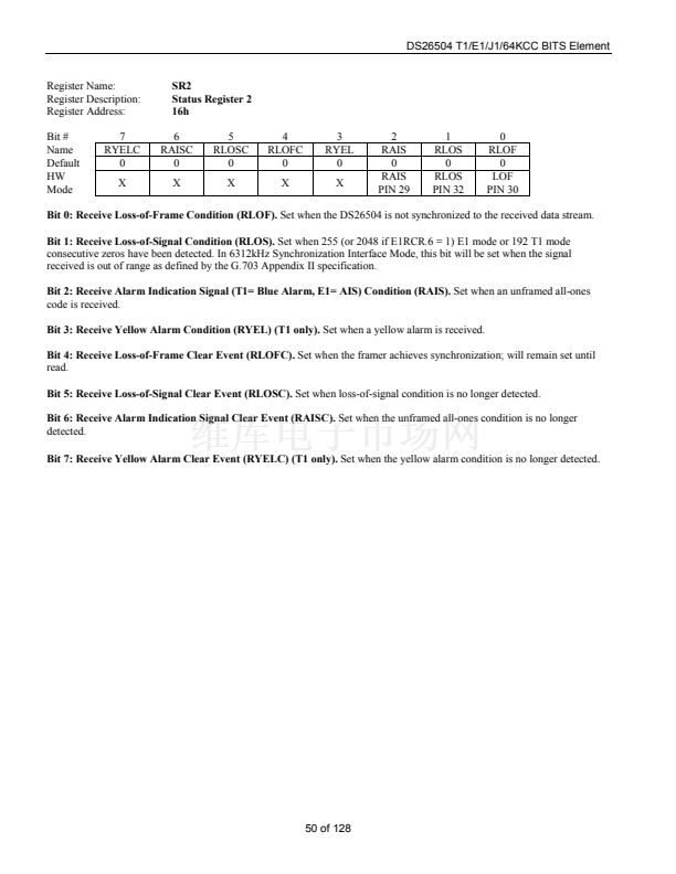
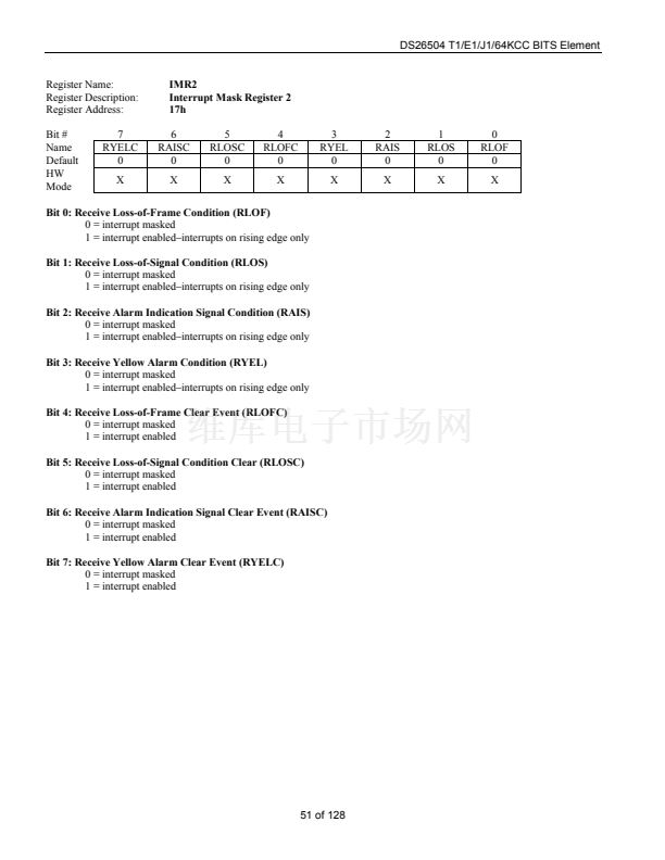
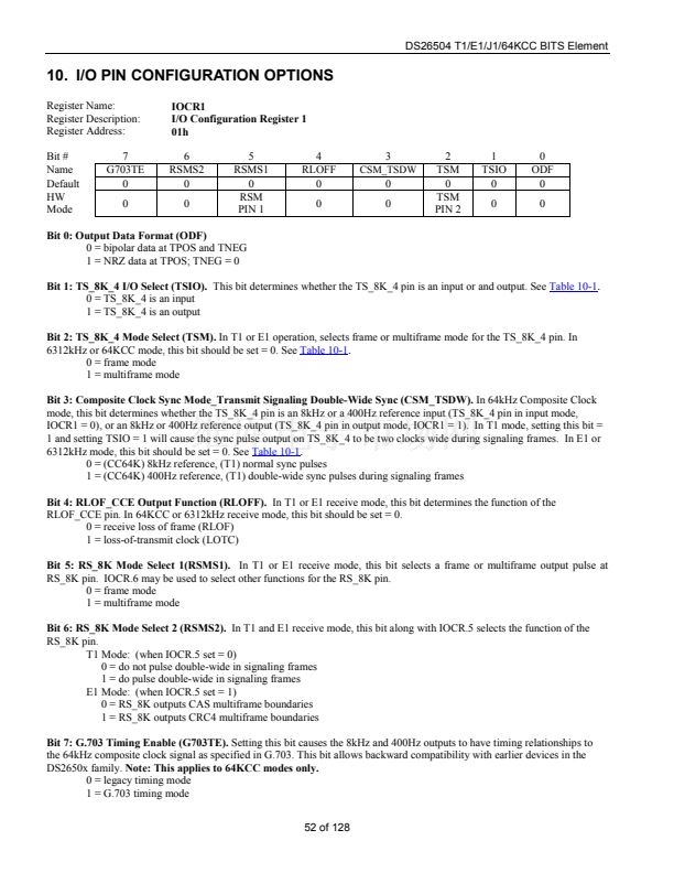
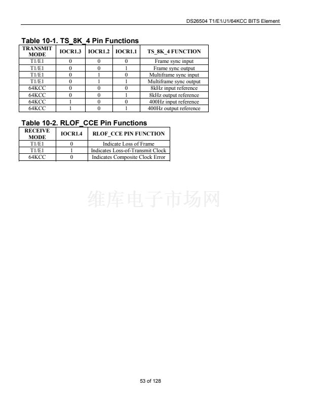
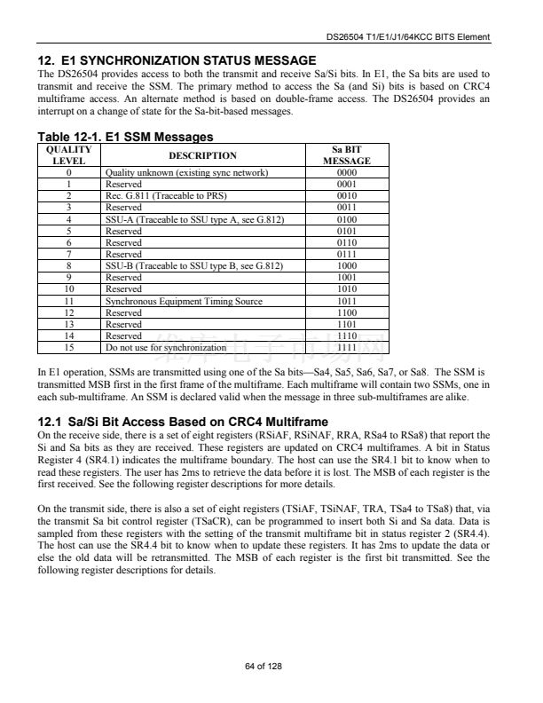
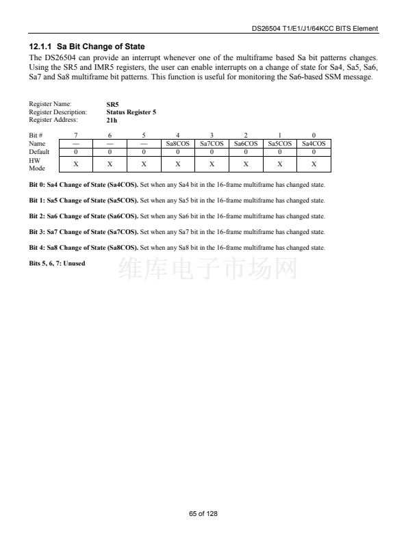
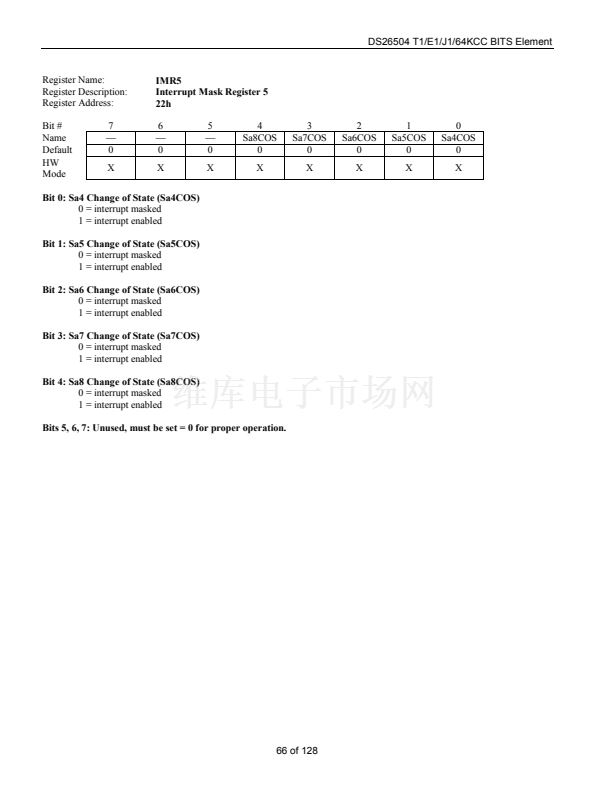
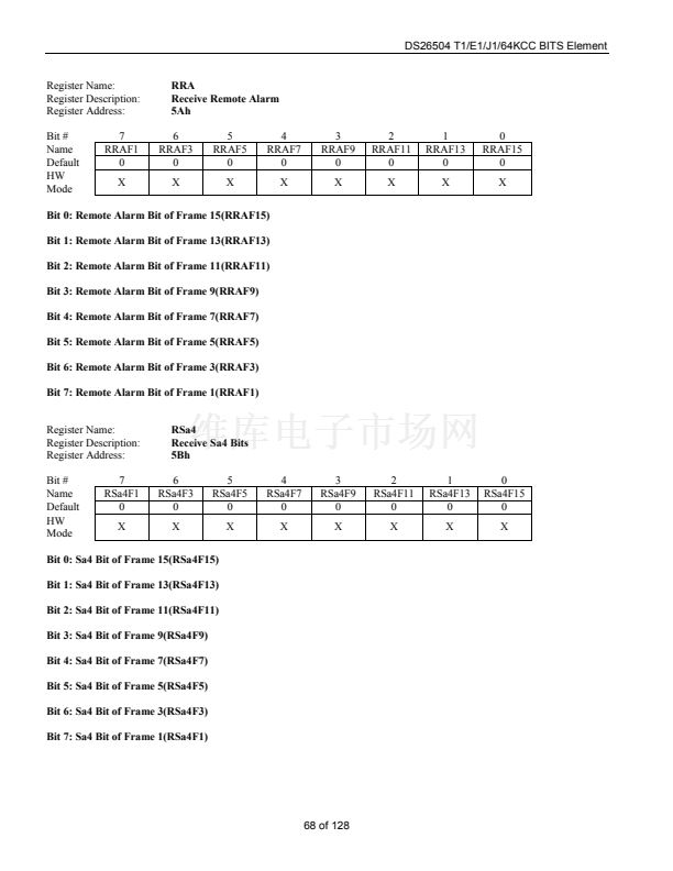
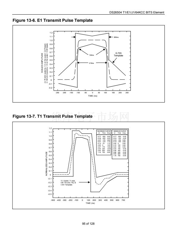
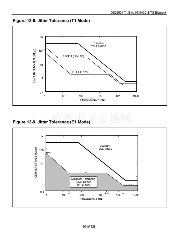
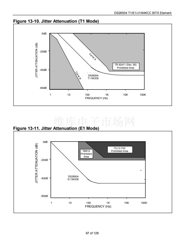
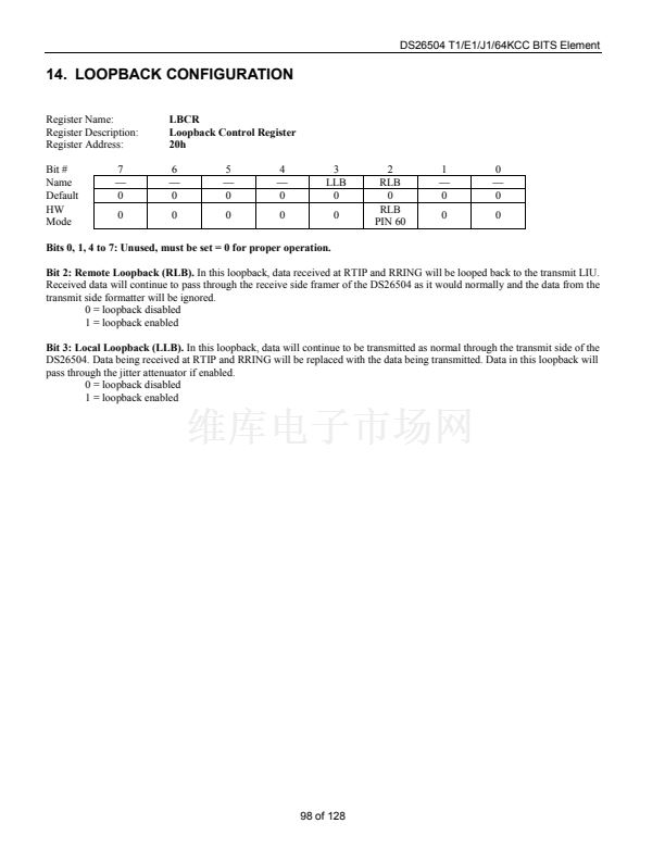
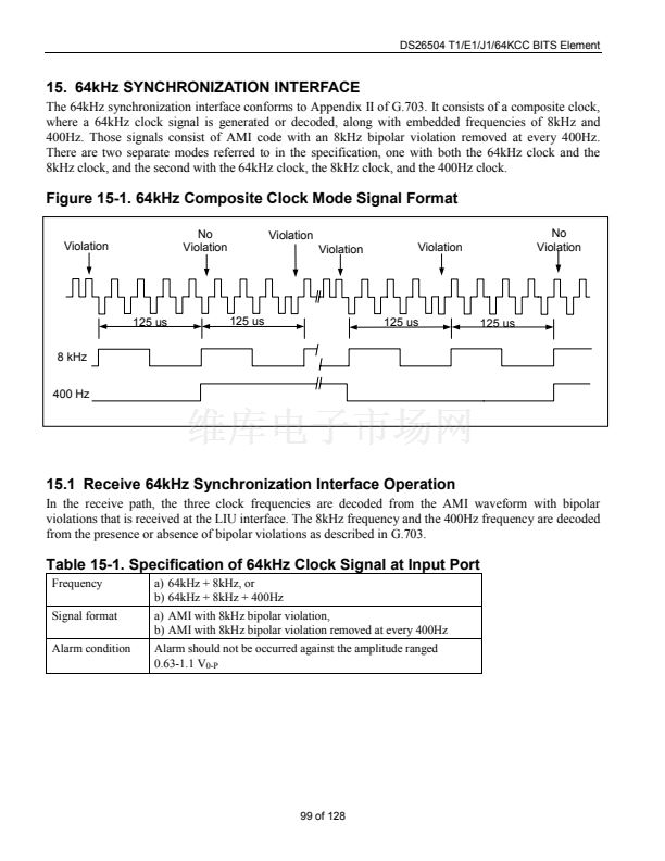
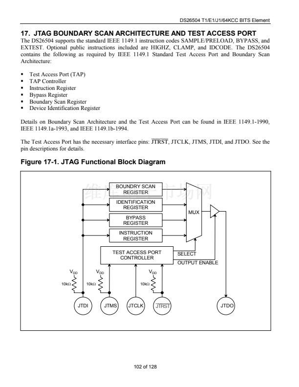
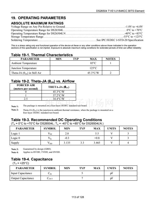
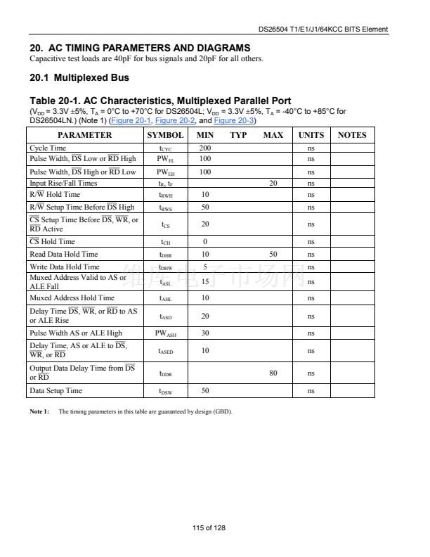
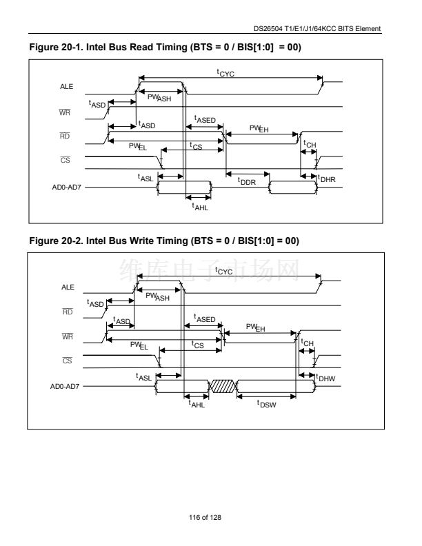
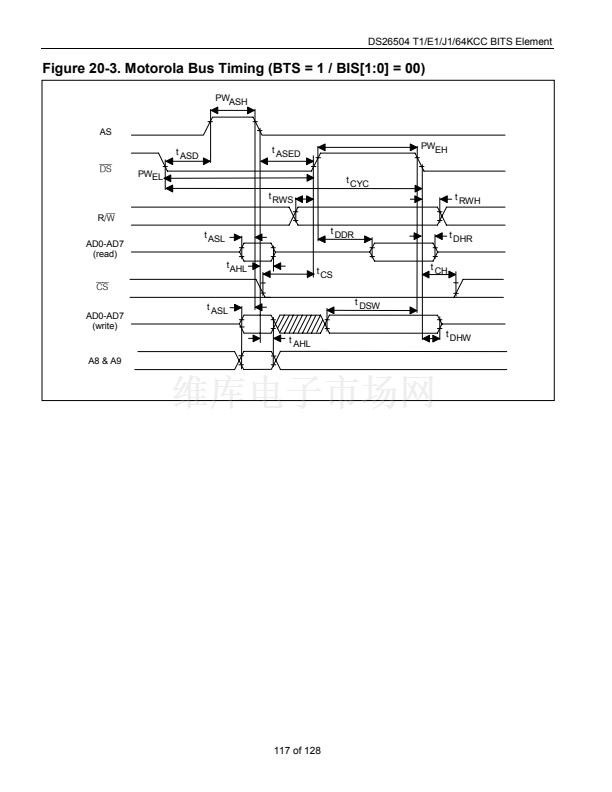
DS26504 T1/E1/J1/64KCC BITS Element
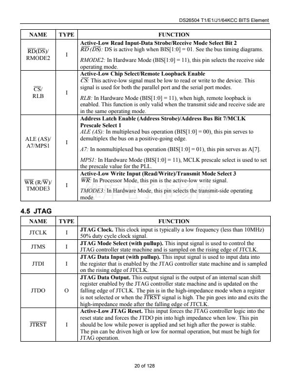
NAME
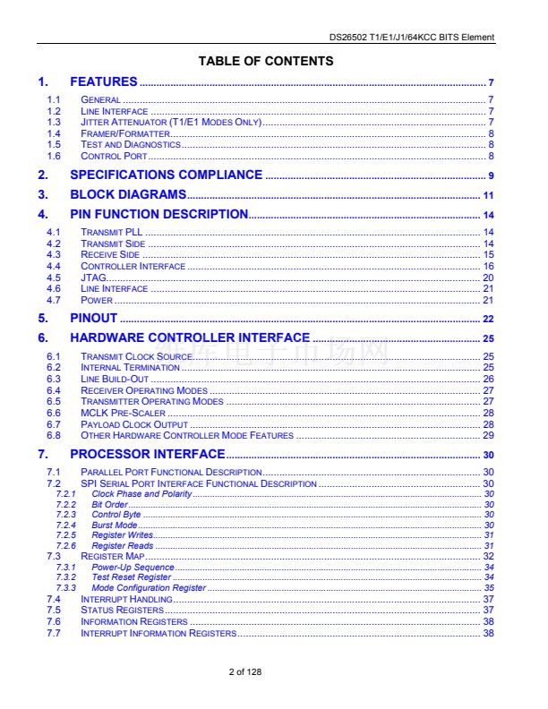
TYPE
A4/CPHA/
L2
I
FUNCTION
Address Bus Bit A[4]/Serial Port Clock Phase Select/Line Build-Out
Select 2
A4:
In nonmultiplexed bus operation (BIS[1:0] = 01), this pin serves as A[4]. In
multiplexed bus operation (BIS[1:0] = 00), these pins are not used and should
be tied low.
CPHA:
In Serial Port Mode (BIS[1:0] = 10), this pin selects the serial port
clock phase. See the functional timing diagrams for the Serial Port Interface.
L2:
In Hardware Mode (BIS[1:0] = 11), this pin selects the line build-out value.
Address Bus Bit A[3]/Line Build-Out Select 1
A3:
In nonmultiplexed bus operation (BIS[1:0] = 01), this pin serves as A[3]. In
multiplexed bus operation (BIS[1:0] = 00), these pins are not used and should
be tied low.
L1:
In Hardware Mode (BIS[1:0] = 11), this pin selects the line build-out value.
Address Bus Bit A[2]/Line Build-Out Select 0
A2:
In nonmultiplexed bus operation (BIS[1:0] = 01), this pin serves as A[2]. In
multiplexed bus operation (BIS[1:0] = 00), these pins are not used and should
be tied low.
L0:
In Hardware Mode (BIS[1:0] = 11), this pin selects the line build-out value.
Address Bus Bit A[1]/Transmit AIS
A1:
In nonmultiplexed bus operation (BIS[1:0] = 01), this pin serves as A[1]. In
multiplexed bus operation (BIS[1:0] = 00), these pins are not used and should
be tied low.
A3/
L1
I
A2/
L0
I
A1/
TAIS
I
TAIS:
When set to 1 and in T1/E1 operating modes, the transmitter transmits an
AIS pattern.
TAIS (64KCC):
When set = 0 and in any 64KCC mode, the device transmits an
all-ones signal without BPVs. When set = 1, normal 64KCC transmission is
enabled.
Address Bus Bit A[0]/E1 Termination Select
A0:
In nonmultiplexed bus operation (BIS[1:0] = 01), this pin serves as A[0]. In
multiplexed bus operation (BIS[1:0] = 00), these pins are not used and should
be tied low.
E1TS:
In Hardware Mode (BIS[1:0] = 11), this pin selects the E1 internal
termination value (0 = 120W, 1 = 75W).
Bus Type Select/Transmit and Receive B8ZS/HDB3 Enable
BTS:
Strap high to select Motorola bus timing; strap low to select Intel bus
timing. This pin controls the function of the
RD
(DS), ALE (AS), and
WR
(R/W) pins. If BTS = 1, then these pins assume the function listed in
parentheses ().
HBE:
In Hardware Mode (BIS[1:0] = 11), this pin enables transmit and receive
B8ZS/HDB3 when in T1/E1 operating modes.
A0/
E1TS
I
BTS/
HBE
I
19 of 128


 1
1
 2
2
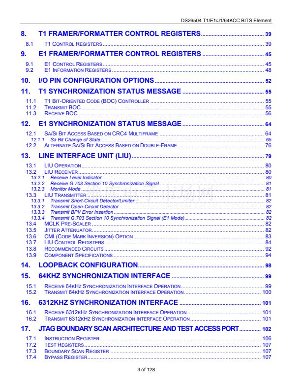 3
3
 4
4
 5
5
 6
6
 7
7
 8
8
 9
9
 10
10
 11
11
 12
12
 13
13
 14
14
 15
15
 16
16
 17
17
 18
18
 19
19
 20
20
 21
21
 22
22
 23
23
 24
24
 25
25
 26
26
 27
27
 28
28
 29
29
 30
30
 31
31
 32
32
 33
33
 34
34
 35
35
 36
36
 37
37
 38
38
 39
39
 40
40
 41
41
 42
42
 43
43
 44
44
 45
45
 46
46
 47
47
 48
48
 49
49
 50
50
 51
51
 52
52
 53
53
 54
54
 55
55
 56
56
 57
57
 58
58
 59
59
 60
60
 61
61
 62
62
 63
63
 64
64
 65
65
 66
66
 67
67
 68
68
 69
69
 70
70
 71
71
 72
72
 73
73
 74
74
 75
75
 76
76
 77
77
 78
78
 79
79
 80
80
 81
81
 82
82
 83
83
 84
84
 85
85
 86
86
 87
87
 88
88
 89
89
 90
90
 91
91
 92
92
 93
93
 94
94
 95
95
 96
96
 97
97
 98
98
 99
99
 100
100
 101
101
 102
102
 103
103
 104
104
 105
105
 106
106
 107
107
 108
108
 109
109
 110
110
 111
111
 112
112
 113
113
 114
114
 115
115
 116
116
 117
117
 118
118
 119
119
 120
120
 121
121
 122
122
 123
123
 124
124
 125
125
 126
126
 127
127
 128
128
