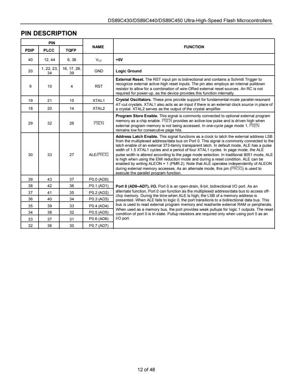
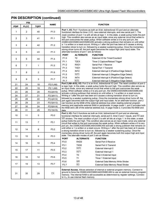
Table 2. SFR Reset Value (continued)
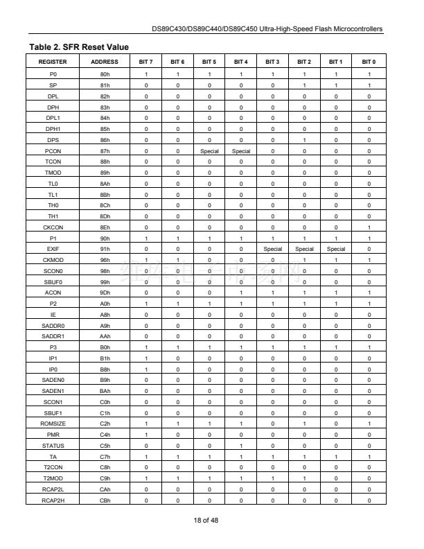
for more information about the bits marked 鈥淪pecial.鈥?/div>
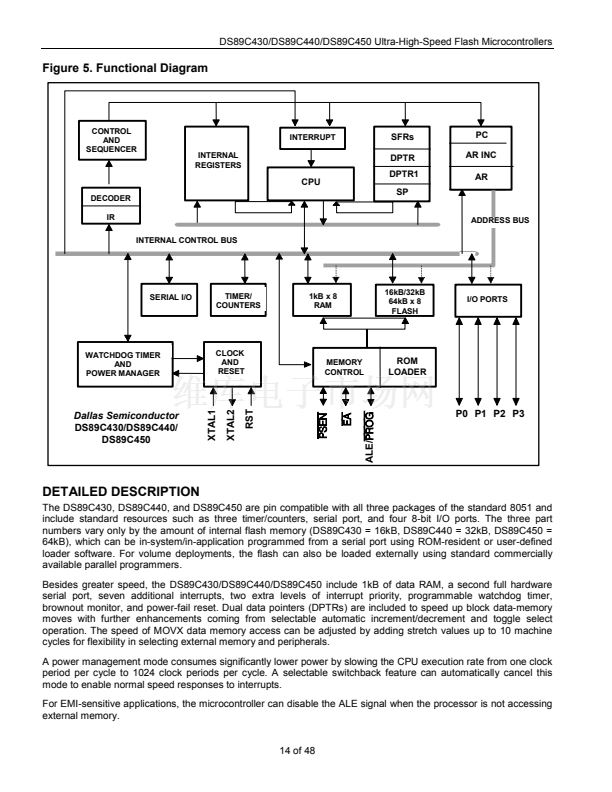
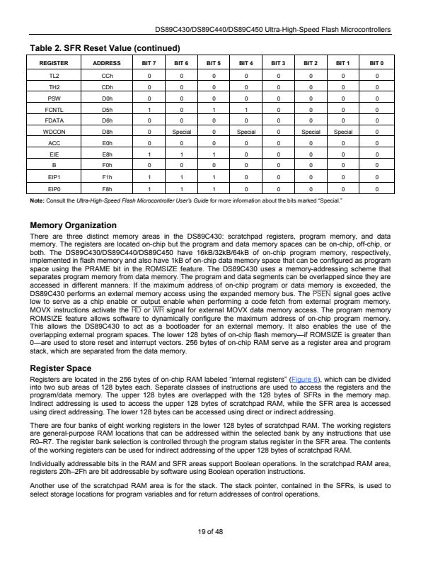
Memory Organization
There are three distinct memory areas in the DS89C430: scratchpad registers, program memory, and data
memory. The registers are located on-chip but the program and data memory spaces can be on-chip, off-chip, or
both. The DS89C430/DS89C440/DS89C450 have 16kB/32kB/64kB of on-chip program memory, respectively,
implemented in flash memory and also have 1kB of on-chip data memory space that can be configured as program
space using the PRAME bit in the ROMSIZE feature. The DS89C430 uses a memory-addressing scheme that
separates program memory from data memory. The program and data segments can be overlapped since they are
accessed in different manners. If the maximum address of on-chip program or data memory is exceeded, the
DS89C430 performs an external memory access using the expanded memory bus. The
PSEN
signal goes active
low to serve as a chip enable or output enable when performing a code fetch from external program memory.
MOVX instructions activate the
RD
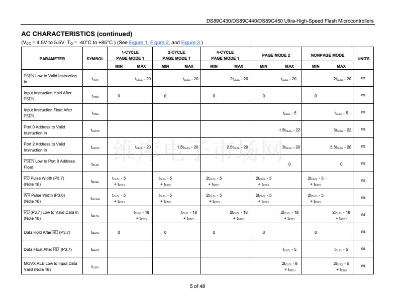
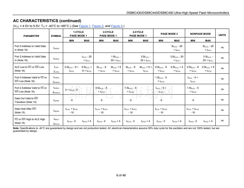
or
WR
signal for external MOVX data memory access. The program memory
ROMSIZE feature allows software to dynamically configure the maximum address of on-chip program memory.
This allows the DS89C430 to act as a bootloader for an external memory. It also enables the use of the
overlapping external program spaces. The lower 128 bytes of on-chip flash memory鈥攊f ROMSIZE is greater than
0鈥攁re used to store reset and interrupt vectors. 256 bytes of on-chip RAM serve as a register area and program
stack, which are separated from the data memory.
Register Space
Registers are located in the 256 bytes of on-chip RAM labeled 鈥渋nternal registers鈥?(Figure
6),
which can be divided
into two sub areas of 128 bytes each. Separate classes of instructions are used to access the registers and the
program/data memory. The upper 128 bytes are overlapped with the 128 bytes of SFRs in the memory map.
Indirect addressing is used to access the upper 128 bytes of scratchpad RAM, while the SFR area is accessed
using direct addressing. The lower 128 bytes can be accessed using direct or indirect addressing.
There are four banks of eight working registers in the lower 128 bytes of scratchpad RAM. The working registers
are general-purpose RAM locations that can be addressed within the selected bank by any instructions that use
R0鈥揜7. The register bank selection is controlled through the program status register in the SFR area. The contents
of the working registers can be used for indirect addressing of the upper 128 bytes of scratchpad RAM.
Individually addressable bits in the RAM and SFR areas support Boolean operations. In the scratchpad RAM area,
registers 20h鈥?Fh are bit addressable by software using Boolean operation instructions.
Another use of the scratchpad RAM area is for the stack. The stack pointer, contained in the SFRs, is used to
select storage locations for program variables and for return addresses of control operations.
19 of 48


 1
1
 2
2
 3
3
 4
4
 5
5
 6
6
 7
7
 8
8
 9
9
 10
10
 11
11
 12
12
 13
13
 14
14
 15
15
 16
16
 17
17
 18
18
 19
19
 20
20
 21
21
 22
22
 23
23
 24
24
 25
25
 26
26
 27
27
 28
28
 29
29
 30
30
 31
31
 32
32
 33
33
 34
34
 35
35
 36
36
 37
37
 38
38
 39
39
 40
40
 41
41
 42
42
 43
43
 44
44
 45
45
 46
46
 47
47
 48
48
