CAUTION: Stresses above those listed in 鈥淎bsolute Maximum Ratings鈥?may cause permanent damage to the device. This is a stress only rating and operation of the
device at these or any other conditions above those indicated in the operational sections of this specification is not implied.
NOTE: All parameters having Min/Max specifications are guaranteed. Typ values are for information purposes only. Unless otherwise noted, all tests are at the specified
temperature and are pulsed tests, therefore: T
J
= T
C
= T
A
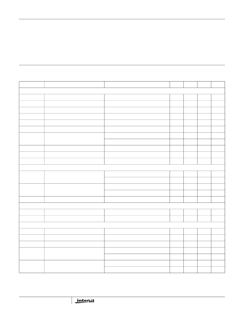
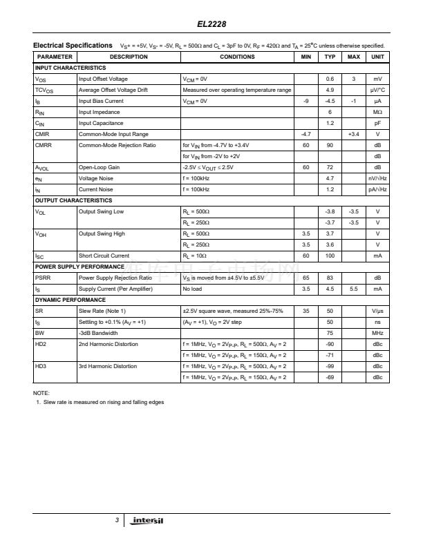
Electrical Specifications
PARAMETER
INPUT CHARACTERISTICS
V
OS
TCV
OS
I
B
R
IN
C
IN
CMIR
CMRR
V
S
+ = +12V, V
S
- = -12V, R
L
= 500鈩?and C
L
= 3pF to 0V, R
F
= 420鈩?and T
A
= 25掳C unless otherwise specified.
CONDITIONS
MIN
TYP
MAX
UNIT
DESCRIPTION
Input Offset Voltage
Average Offset Voltage Drift
Input Bias Current
Input Impedance
Input Capacitance
Common-Mode Input Range
Common-Mode Rejection Ratio
V
CM
= 0V
Measured over operating temperature range
V
CM
= 0V
-9
0.2
-4
-4.5
8
1
-11.8
3
mV
碌V/掳C
-1
碌A
M鈩?/div>
pF
+10.4
90
75
75
4.9
1.2
V
dB
dB
dB
nV/鈭欻z
pA/鈭欻z
for V
IN
from -11.8V to +10.4V
for V
IN
from -10V to +10V
60
60
60
A
VOL
e
N
i
N
Open-Loop Gain
Voltage Noise
Current Noise
-5V
鈮?/div>
V
OUT
鈮?/div>
5V
f = 100kHz
f = 100kHz
OUTPUT CHARACTERISTICS
V
OL
Output Swing Low
R
L
= 500鈩?/div>
R
L
= 250鈩?/div>
V
OH
Output Swing High
R
L
= 500鈩?/div>
R
L
= 250鈩?/div>
I
SC
Short Circuit Current
R
L
= 10鈩?/div>
10
9.5
140
-10.3
-9.5
10.3
10
180
-10
-9
V
V
V
V
mA
POWER SUPPLY PERFORMANCE
PSRR
I
S
Power Supply Rejection Ratio
Supply Current (per Amplifier)
V
S
is moved from 卤10.8V to 卤13.2V
No load
65
4
83
5
6
dB
mA
DYNAMIC PERFORMANCE
SR
t
S
BW
HD2
Slew Rate (Note 1)
Settling to +0.1% (A
V
= +1)
-3dB Bandwidth
2nd Harmonic Distortion
f = 1MHz, V
O
= 2V
P-P
, R
L
= 500鈩? A
V
= 2
f = 1MHz, V
O
= 2V
P-P
, R
L
= 150鈩? A
V
= 2
HD3
3rd Harmonic Distortion
f = 1MHz, V
O
= 2V
P-P
, R
L
= 500鈩? A
V
= 2
f = 1MHz, V
O
= 2V
P-P
, R
L
= 150鈩? A
V
= 2
NOTE:
1. Slew rate is measured on rising and falling edges


 1
1
 2
2
 3
3
 4
4
 5
5
 6
6
 7
7
 8
8
 9
9
 10
10
