ICL7660, ICL7660A
V+
1
2
C
1
+
ICL7660
ICL7660A
8
7
6
5
C
OSC
+
1
2
C
1
ICL7660
ICL7660A
8
7
6
5
V
OUT
= (2V+)
-
(V
FD1
)
-
(V
FD2
)
+
V+
V
OUT
=
-
(nV
IN
- V
FDX
)
-
D
1
+
C
3
-
3
4
-
3
4
-
+
V
OUT
C
2
-
C
2
+
D
2
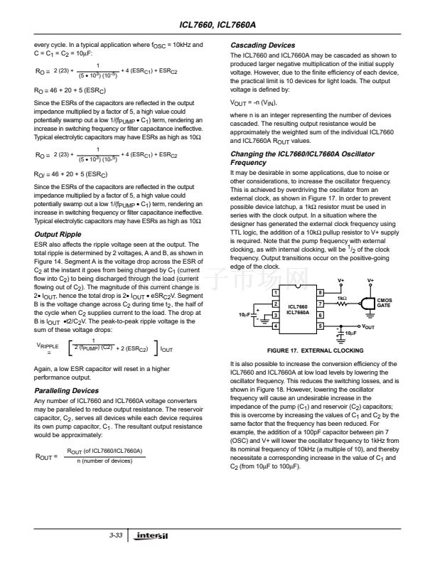
FIGURE 18. LOWERING OSCILLATOR FREQUENCY
-
C
4
Positive Voltage Doubling
The ICL7660 and ICL7660A may be employed to achieve
positive voltage doubling using the circuit shown in Figure
19. In this application, the pump inverter switches of the
ICL7660 and ICL7660A are used to charge C
1
to a voltage
level of V+ -V
F
(where V+ is the supply voltage and V
F
is the
forward voltage drop of diode D
1
). On the transfer cycle, the
voltage on C
1
plus the supply voltage (V+) is applied through
diode D
2
to capacitor C
2
. The voltage thus created on C
2
becomes (2V+) - (2VF) or twice the supply voltage minus the
combined forward voltage drops of diodes D
1
and D
2
.
The source impedance of the output (V
OUT
) will depend on
the output current, but for V+ = 5V and an output current of
10mA it will be approximately 60鈩?
V+
1
2
3
4
ICL7660
ICL7660A
8
7
6
5
+
+
C
1
D
1
D
2
V
OUT
=
(2V+) - (2V
F
)
FIGURE 20. COMBINED NEGATIVE VOLTAGE CONVERTER
AND POSITIVE DOUBLER
Voltage Splitting
The bidirectional characteristics can also be used to split a
higher supply in half, as shown in Figure 21. The combined
load will be evenly shared between the two sides. Because
the switches share the load in parallel, the output impedance
is much lower than in the standard circuits, and higher
currents can be drawn from the device. By using this circuit,
and then the circuit of Figure 16, +15V can be converted (via
+7.5, and -7.5) to a nominal -15V, although with rather high
series output resistance (
~
250鈩?.
V+
+
R
L1
50碌F
-
1
8
ICL7660
ICL7660A
7
6
5
2
V
OUT
= V+ - V-
2
R
L2
50碌F
+
-
+
3
4
-
-
C
2
50碌F
-
V
-
FIGURE 19. POSITIVE VOLT DOUBLER
FIGURE 21. SPLITTING A SUPPLY IN HALF
Combined Negative Voltage Conversion
and Positive Supply Doubling
Figure 20 combines the functions shown in Figures 13 and
Figure 19 to provide negative voltage conversion and
positive voltage doubling simultaneously. This approach
would be, for example, suitable for generating +9V and -5V
from an existing +5V supply. In this instance capacitors C
1
and C
3
perform the pump and reservoir functions
respectively for the generation of the negative voltage, while
capacitors C
2
and C
4
are pump and reservoir respectively
for the doubled positive voltage. There is a penalty in this
con铿乬uration which combines both functions, however, in
that the source impedances of the generated supplies will be
somewhat higher due to the 铿乶ite impedance of the common
charge pump driver at pin 2 of the device.
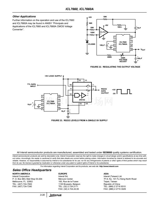
Regulated Negative Voltage Supply
In some cases, the output impedance of the ICL7660 and
ICL7660A can be a problem, particularly if the load current
varies substantially. The circuit of Figure 22 can be used to
overcome this by controlling the input voltage, via an ICL7611
low-power CMOS op amp, in such a way as to maintain a
nearly constant output voltage. Direct feedback is inadvisable,
since the ICL7660s and ICL7660As output does not respond
instantaneously to change in input, but only after the switching
delay. The circuit shown supplies enough delay to
accommodate the ICL7660 and ICL7660A, while maintaining
adequate feedback. An increase in pump and storage
capacitors is desirable, and the values shown provides an
output impedance of less than 5鈩?to a load of 10mA.
3-34


 1
1
 2
2
 3
3
 4
4
 5
5
 6
6
 7
7
 8
8
 9
9
 10
10
