(EQ. 23)
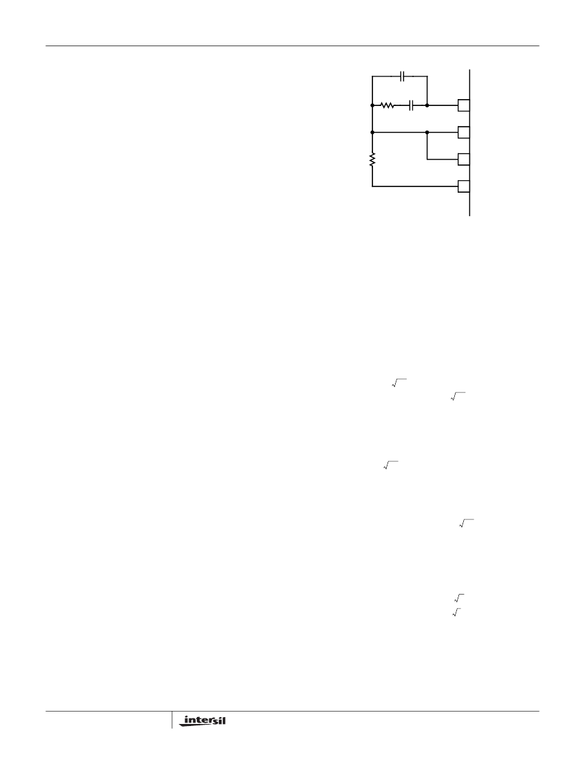
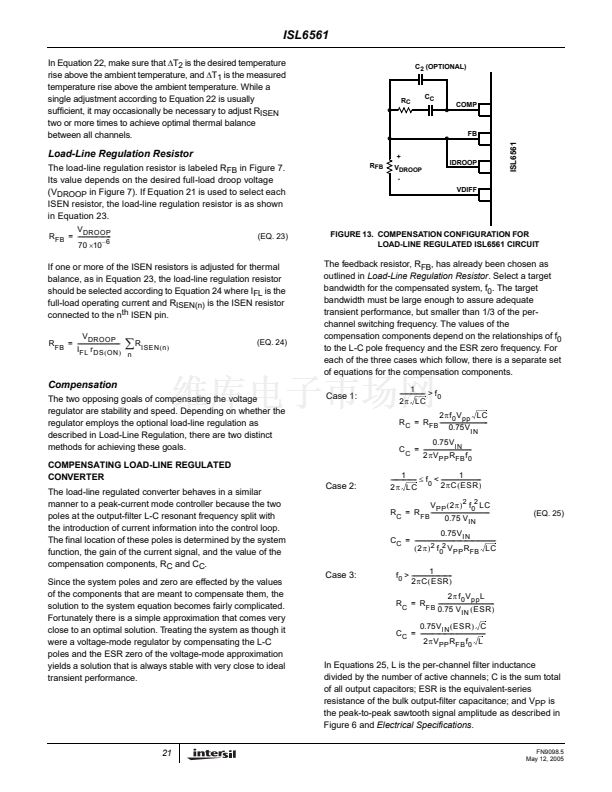
FIGURE 13. COMPENSATION CONFIGURATION FOR
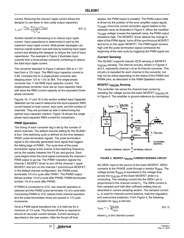
ISEN pin.
鈭?/div>
R
ISEN
(
n
)
n
(EQ. 24)
The feedback resistor, R
FB
, has already been chosen as
outlined in
Load-Line Regulation Resistor.
Select a target
bandwidth for the compensated system, f
0
. The target
bandwidth must be large enough to assure adequate
transient performance, but smaller than 1/3 of the per-
channel switching frequency. The values of the
compensation components depend on the relationships of f
0
to the L-C pole frequency and the ESR zero frequency. For
each of the three cases which follow, there is a separate set
of equations for the compensation components.
Case 1:
1
------------------- > f
0
2蟺 LC
2蟺f
0
V
pp
LC
-
R
C
= R
FB
-----------------------------------
0.75V
IN
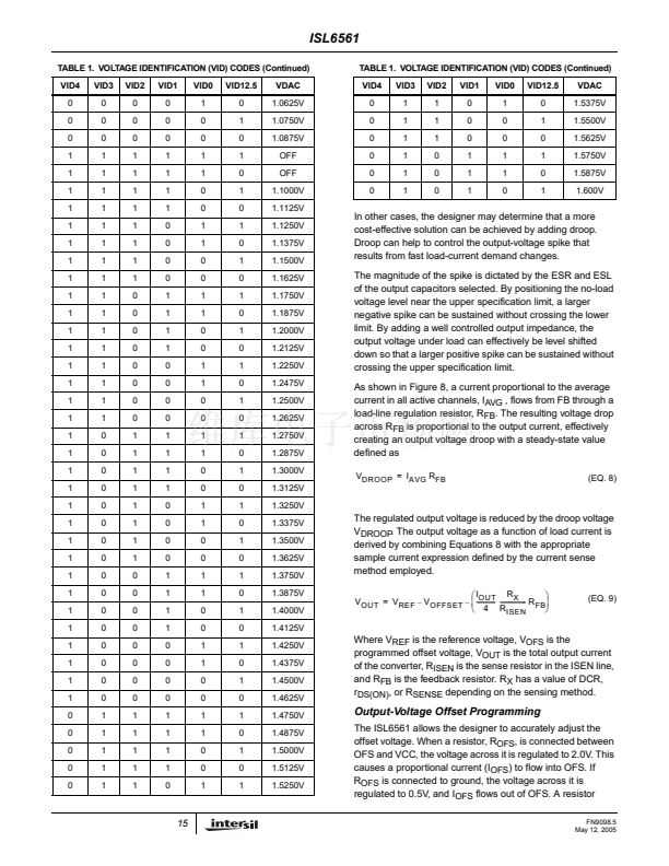
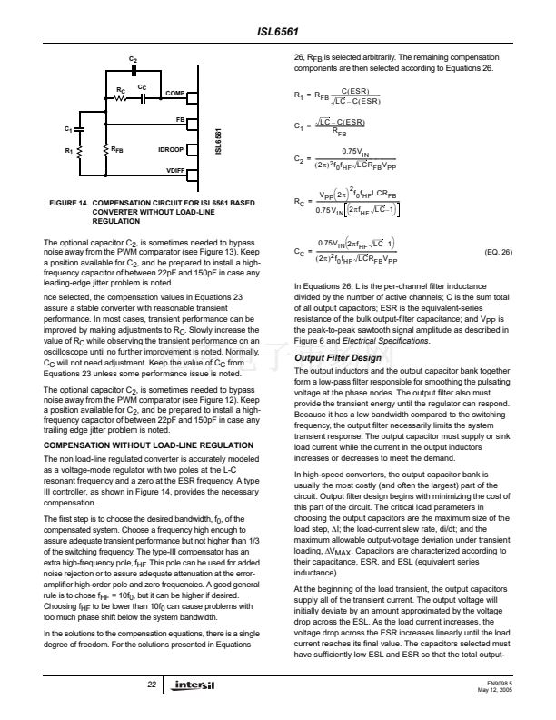
Compensation
The two opposing goals of compensating the voltage
regulator are stability and speed. Depending on whether the
regulator employs the optional load-line regulation as
described in Load-Line Regulation, there are two distinct
methods for achieving these goals.
COMPENSATING LOAD-LINE REGULATED
CONVERTER
The load-line regulated converter behaves in a similar
manner to a peak-current mode controller because the two
poles at the output-filter L-C resonant frequency split with
the introduction of current information into the control loop.
The final location of these poles is determined by the system
function, the gain of the current signal, and the value of the
compensation components, R
C
and C
C
.
Since the system poles and zero are effected by the values
of the components that are meant to compensate them, the
solution to the system equation becomes fairly complicated.
Fortunately there is a simple approximation that comes very
close to an optimal solution. Treating the system as though it
were a voltage-mode regulator by compensating the L-C
poles and the ESR zero of the voltage-mode approximation
yields a solution that is always stable with very close to ideal
transient performance.
Case 2:
0.75V
IN
-
C
C
= -----------------------------------
2蟺V
PP
R
FB
f
0
1
1
-------------------
鈮?/div>
f
0
< -----------------------------
-
2蟺C
(
ESR
)
2蟺 LC
V
PP
(
2蟺
)
2
f
02
LC
R
C
= R
FB
--------------------------------------------
0.75 V
IN
ISL6561
(EQ. 25)
FN9098.5
May 12, 2005
0.75V
IN
-
C
C
= ------------------------------------------------------------
(
2蟺
)
2
f
02
V
PP
R
FB
LC
Case 3:
1
f
0
> -----------------------------
-
2蟺C
(
ESR
)
2蟺 f
0
V
pp
L
-
R
C
= R
FB
-----------------------------------------
0.75 V
IN
(
ESR
)
0.75V
IN
(
ESR
)
C
-
C
C
= ------------------------------------------------
2蟺V
PP
R
FB
f
0
L
In Equations 25, L is the per-channel filter inductance
divided by the number of active channels; C is the sum total
of all output capacitors; ESR is the equivalent-series
resistance of the bulk output-filter capacitance; and V
PP
is
the peak-to-peak sawtooth signal amplitude as described in
Figure 6 and
Electrical Specifications.
21


 1
1
 2
2
 3
3
 4
4
 5
5
 6
6
 7
7
 8
8
 9
9
 10
10
 11
11
 12
12
 13
13
 14
14
 15
15
 16
16
 17
17
 18
18
 19
19
 20
20
 21
21
 22
22
 23
23
 24
24
 25
25
 26
26
