3.9鈩?/div>
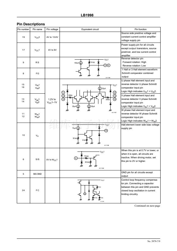
VCC2
18
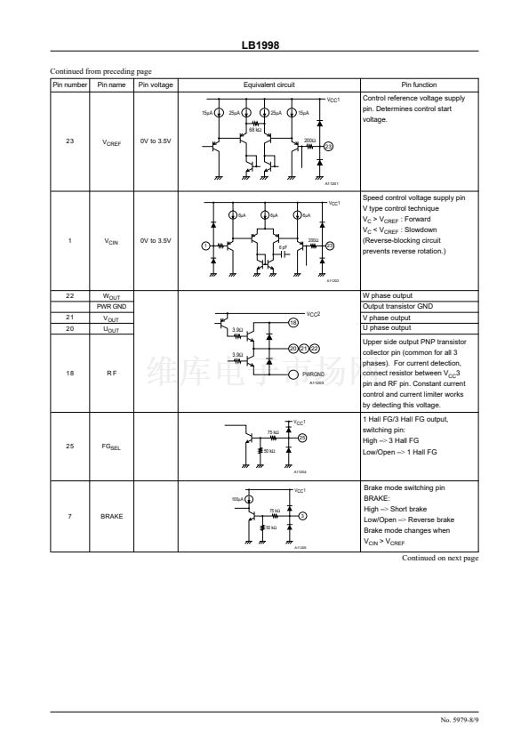
W phase output
Output transistor GND
V phase output
U phase output
Upper side output PNP transistor
collector pin (common for all 3
phases). For current detection,
connect resistor between V
CC
3
pin and RF pin. Constant current
control and current limiter works
by detecting this voltage.
VCC1
75 k鈩?/div>
25
18
RF
PWRGND
A11203
1 Hall FG/3 Hall FG output,
switching pin:
High 鈥?gt; 3 Hall FG
Low/Open 鈥?gt; 1 Hall FG
25
FG
SEL
50 k鈩?/div>
A11204
VCC1
100碌A
75 k鈩?/div>
Brake mode switching pin
BRAKE:
High 鈥?gt; Short brake
Low/Open 鈥?gt; Reverse brake
Brake mode changes when
V
CIN
> V
CREF
.
7
BRAKE
50 k鈩?/div>
3
A11205
Continued on next page
No. 5979-8/9


 1
1
 2
2
 3
3
 4
4
 5
5
 6
6
 7
7
 8
8
 9
9
