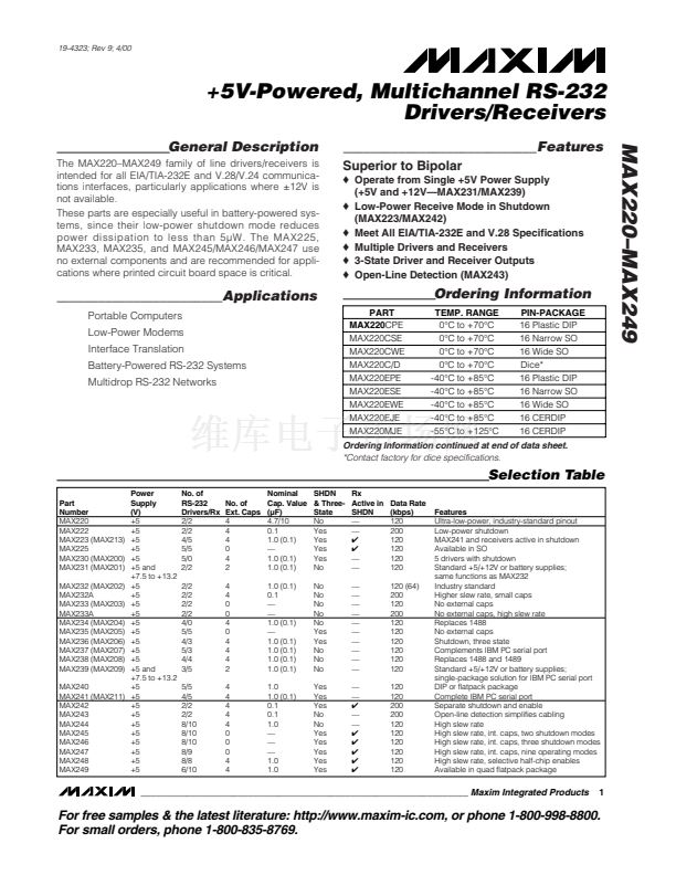
+5V-Powered, Multichannel RS-232
Drivers/Receivers
MAX220鈥揗AX249
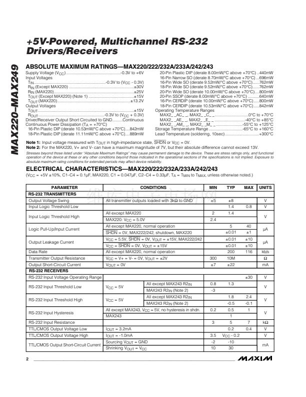
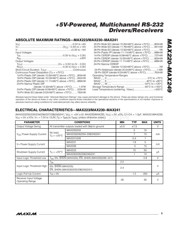
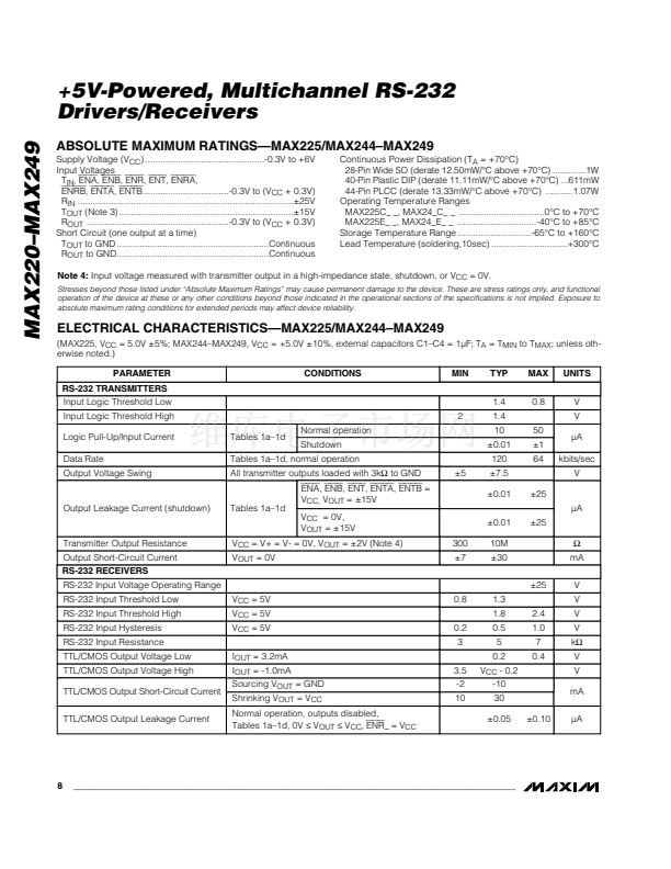
ABSOLUTE MAXIMUM RATINGS鈥擬AX220/222/232A/233A/242/243
Supply Voltage (V
CC
) ...............................................-0.3V to +6V
Input Voltages
T
IN
..............................................................-0.3V to (V
CC
- 0.3V)
R
IN
(Except MAX220) ........................................................卤30V
R
IN
(MAX220).....................................................................卤25V
T
OUT
(Except MAX220) (Note 1) .......................................卤15V
T
OUT
(MAX220)...............................................................卤13.2V
Output Voltages
T
OUT
...................................................................................卤15V
R
OUT
.........................................................-0.3V to (V
CC
+ 0.3V)
Driver/Receiver Output Short Circuited to GND.........Continuous
Continuous Power Dissipation (T
A
= +70掳C)
16-Pin Plastic DIP (derate 10.53mW/掳C above +70掳C)....842mW
18-Pin Plastic DIP (derate 11.11mW/掳C above +70掳C)....889mW
20-Pin Plastic DIP (derate 8.00mW/掳C above +70掳C) ..440mW
16-Pin Narrow SO (derate 8.70mW/掳C above +70掳C) ...696mW
16-Pin Wide SO (derate 9.52mW/掳C above +70掳C)......762mW
18-Pin Wide SO (derate 9.52mW/掳C above +70掳C)......762mW
20-Pin Wide SO (derate 10.00mW/掳C above +70掳C)....800mW
20-Pin SSOP (derate 8.00mW/掳C above +70掳C) ..........640mW
16-Pin CERDIP (derate 10.00mW/掳C above +70掳C).....800mW
18-Pin CERDIP (derate 10.53mW/掳C above +70掳C).....842mW
Operating Temperature Ranges
MAX2_ _AC_ _, MAX2_ _C_ _ .............................0掳C to +70掳C
MAX2_ _AE_ _, MAX2_ _E_ _ ..........................-40掳C to +85掳C
MAX2_ _AM_ _, MAX2_ _M_ _ .......................-55掳C to +125掳C
Storage Temperature Range .............................-65掳C to +160掳C
Lead Temperature (soldering, 10sec) .............................+300掳C
Note 1:
Input voltage measured with T
OUT
in high-impedance state,
SHDN
or V
CC
= 0V.
Note 2:
For the MAX220, V+ and V- can have a maximum magnitude of 7V, but their absolute difference cannot exceed 13V.
Stresses beyond those listed under 鈥淎bsolute Maximum Ratings鈥?may cause permanent damage to the device. These are stress ratings only, and functional
operation of the device at these or any other conditions beyond those indicated in the operational sections of the specifications is not implied. Exposure to
absolute maximum rating conditions for extended periods may affect device reliability.
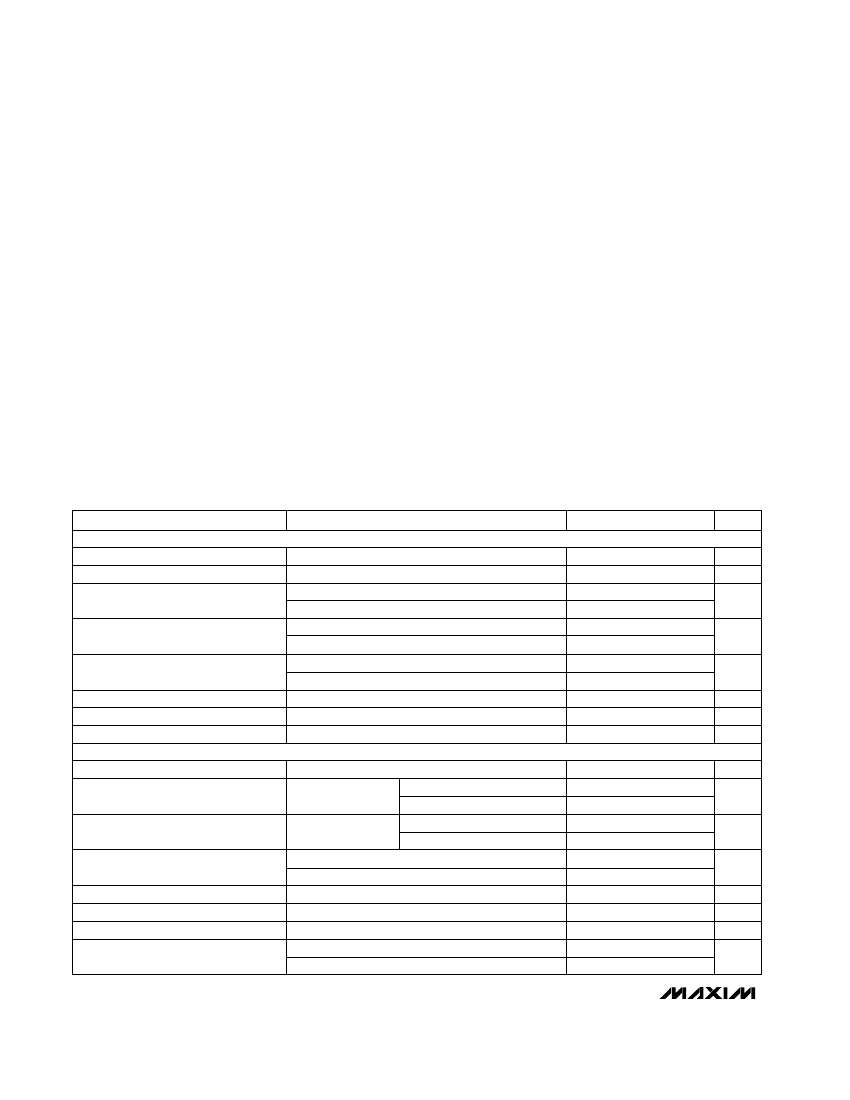
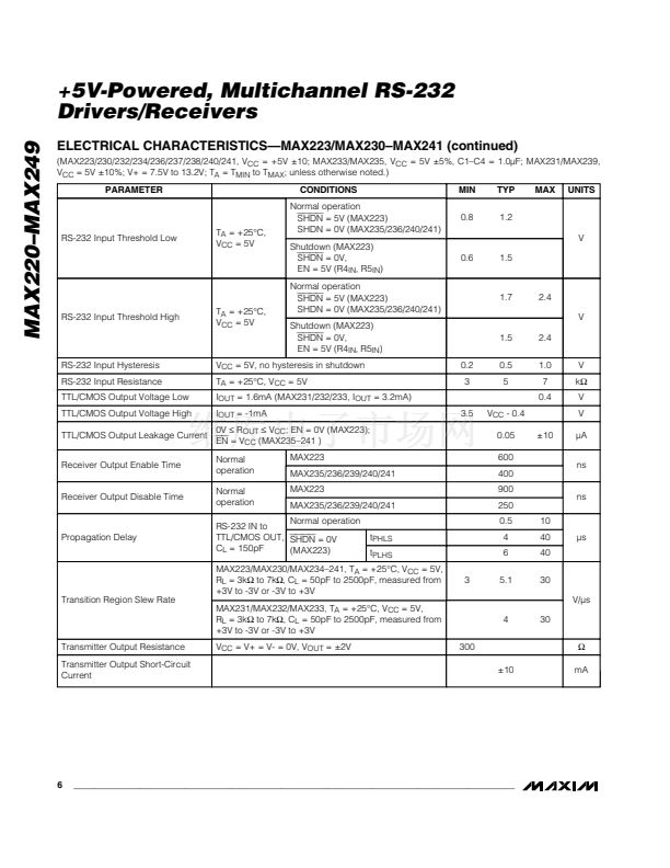
ELECTRICAL CHARACTERISTICS鈥擬AX220/222/232A/233A/242/243
(V
CC
= +5V 卤10%, C1鈥揅4 = 0.1碌F鈥?MAX220, C1 = 0.047碌F, C2鈥揅4 = 0.33碌F, T
A
= T
MIN
to T
MAX
鈥?unless otherwise noted.)
PARAMETER
RS-232 TRANSMITTERS
Output Voltage Swing
Input Logic Threshold Low
Input Logic Threshold High
Logic Pull-Up/lnput Current
Output Leakage Current
Data Rate
Transmitter Output Resistance
Output Short-Circuit Current
RS-232 RECEIVERS
RS-232 Input Voltage Operating Range
RS-232 Input Threshold Low
RS-232 Input Threshold High
RS-232 Input Hysteresis
RS-232 Input Resistance
TTL/CMOS Output Voltage Low
TTL/CMOS Output Voltage High
TTL/CMOS Output Short-Circuit Current
I
OUT
= 3.2mA
I
OUT
= -1.0mA
Sourcing V
OUT
= GND
Shrinking V
OUT
= V
CC
3.5
-2
10
V
CC
= 5V
V
CC
= 5V
All except MAX243 R2
IN
MAX243 R2
IN
(Note 2)
All except MAX243 R2
IN
MAX243 R2
IN
(Note 2)
0.2
3
0.8
-3
1.8
-0.5
0.5
1
5
0.2
V
CC
- 0.2
-10
30
7
0.4
2.4
-0.1
1
1.3
卤30
V
V
V
V
k鈩?/div>
V
V
mA
All except MAX220
MAX220: V
CC
= 5.0V
All except MAX220, normal operation
SHDN
= 0V, MAX222/242, shutdown, MAX220
V
CC
= 5.5V,
SHDN
= 0V, V
OUT
= 卤15V, MAX222/242
V
CC
=
SHDN
= 0V, V
OUT
= 卤15V
All except MAX220, normal operation
V
CC
= V+ = V- = 0V, V
OUT
= 卤2V
V
OUT
= 0V
300
卤7
2
2.4
5
卤0.01
卤0.01
卤0.01
200
10M
卤22
40
卤1
卤10
卤10
116
All transmitter outputs loaded with 3k鈩?to GND
卤5
卤8
1.4
1.4
0.8
V
V
V
碌A
碌A
kb/s
鈩?/div>
mA
CONDITIONS
MIN
TYP
MAX
UNITS
All except MAX243, V
CC
= 5V, no hysteresis in shdn.
MAX243
2
_______________________________________________________________________________________


 1
1
 2
2
 3
3
 4
4
 5
5
 6
6
 7
7
 8
8
 9
9
 10
10
 11
11
 12
12
 13
13
 14
14
 15
15
 16
16
 17
17
 18
18
 19
19
 20
20
 21
21
 22
22
 23
23
 24
24
 25
25
 26
26
 27
27
 28
28
 29
29
 30
30
 31
31
 32
32
 33
33
 34
34
 35
35
 36
36
