Low-Cost, Low-Power, 8-Bit DACs with
2-Wire Serial Interface in SOT23
MAX5380/MAX5381/MAX5382
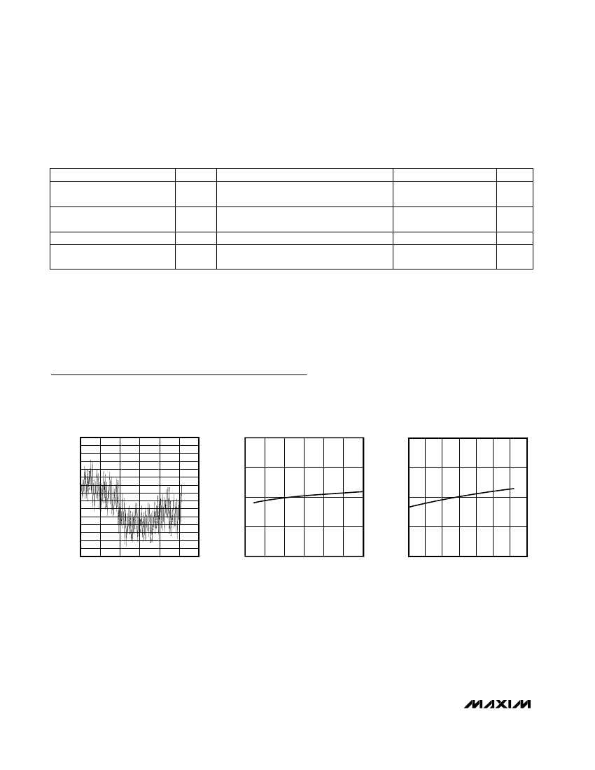
TIMING CHARACTERISTICS (continued)
(Figure 3; V
DD
= +2.7V to +3.6V (MAX5380), V
DD
= +4.5V to +5.5V (MAX5381), V
DD
= +2.7V to +5.5V (MAX5382); R
L
= 10k鈩?
C
L
= 50pF, T
A
= T
MIN
to T
MAX
, unless otherwise noted. Typical values are T
A
= +25掳C.) (Note 7)
PARAMETER
Rise Time of Both SDA and
SCL Signals
Fall Time of Both SDA and
SCL Signals
Setup Time for STOP Condition
Capacitive Load for Each
Bus Line
Note 1:
Note 2:
Note 3:
Note 4:
Note 5:
Note 6:
Note 7:
SYMBOL
t
r
t
f
t
SU:STO
C
b
0.6
400
CONDITIONS
MIN
TYP
MAX
300
300
UNITS
ns
ns
碌s
pF
Guaranteed from code 5 to code 255.
The offset value extrapolated from the range over which the INL is guaranteed.
MAX5382 tested at V
DD
= +5V 卤10%.
MAX5380 tested at V
DD
= +3V 卤10%, MAX5381 tested at V
DD
= 5V 卤10%.
Actual output voltages at full scale are 255/256 x V
REF
.
Output settling time is measured by taking the code from code 5 to 255, and from code 255 to 5.
Guaranteed by design.
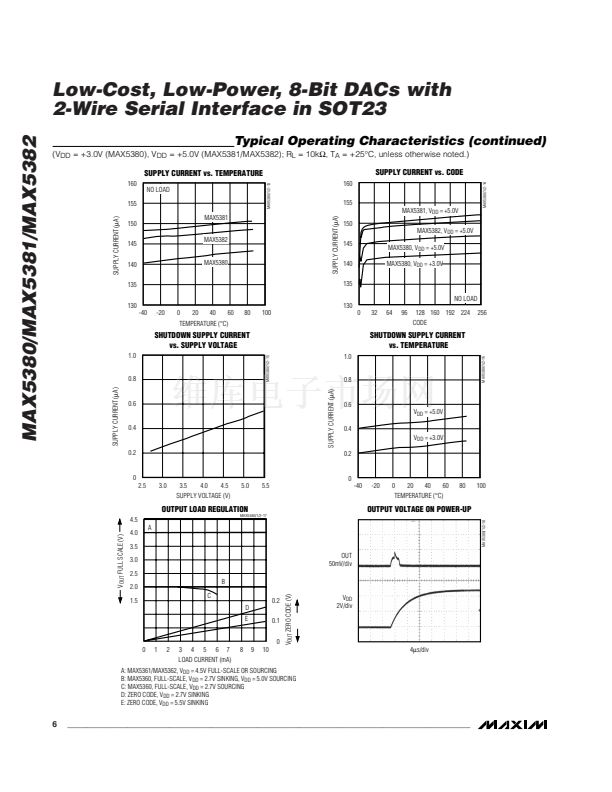
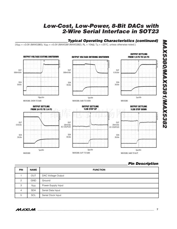
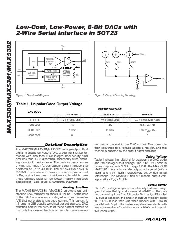
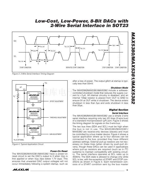
Typical Operating Characteristics
(V
DD
= +3.0V (MAX5380), V
DD
= +5.0V (MAX5381/MAX5382); R
L
= 10k鈩? T
A
= +25掳C, unless otherwise noted.)
INTEGRAL NONLINEARITY vs. CODE
MAX5380/1/2-01
INTEGRAL NONLINEARITY
vs. SUPPLY VOLTAGE
MAX5380/1/2-02
INTEGRAL NONLINEARITY
vs. TEMPERATURE
MAX5380/1/2-03
0.075
0.050
0.025
0
0
-0.05
INL (LSB)
INL (LSB)
-0.05
INL (LSB)
0
-0.025
-0.050
-0.075
-0.100
-0.10
-0.10
-0.15
-0.15
-0.20
0
50
100
150
CODE
200
250
300
2.5
3.0
3.5
4.0
4.5
5.0
5.5
SUPPLY VOLTAGE (V)
-0.20
-40
-20
0
20
40
60
80
100
TEMPERATURE (掳C)
4
_______________________________________________________________________________________


 1
1
 2
2
 3
3
 4
4
 5
5
 6
6
 7
7
 8
8
 9
9
 10
10
 11
11
 12
12
