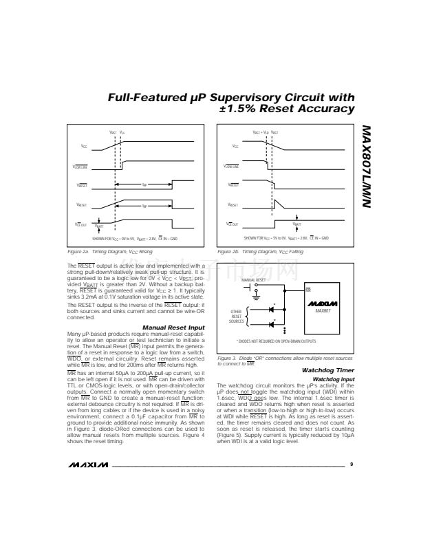
Full-Featured 碌P Supervisory Circuit with
卤1.5% Reset Accuracy
MAX807L/M/N
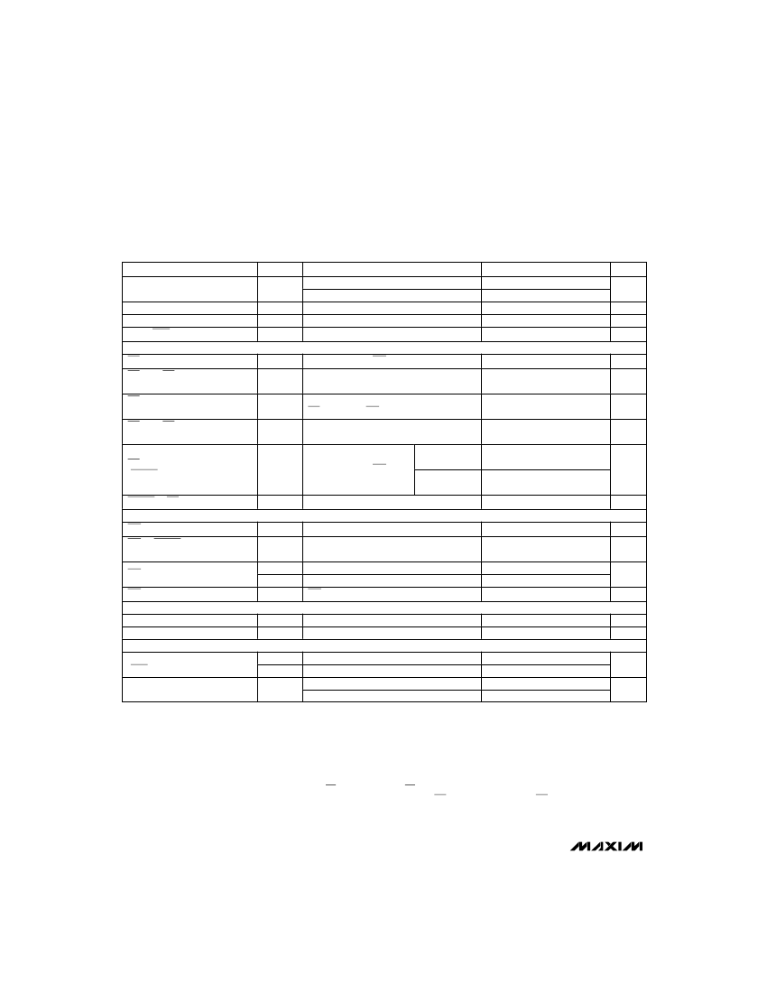
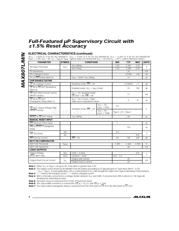
ELECTRICAL CHARACTERISTICS (continued)
(V
CC
= 4.60V to 5.5V for the MAX807L, V
CC
= 4.50V to 5.5V for the MAX807N, V
CC
= 4.35V to 5.5V for the MAX807M,
V
BATT
= 2.8V, V
PFI
= 0V, T
A
= T
MIN
to T
MAX
. Typical values are tested with V
CC
= 5V and T
A
= +25掳C, unless otherwise noted.)
PARAMETER
PFI Input Threshold
PFI Hysteresis
PFI Leakage Current
PFI to PFO Delay (Note 5)
CHIP-ENABLE GATING
CE IN Leakage Current
CE IN to CE OUT Resistance
(Note 6)
CE OUT Short-Circuit Current
(RESET active)
CE IN to CE OUT
Propagation Delay (Note 7)
CE OUT Output Voltage High
(RESET active)
RESET to CE OUT Delay
MANUAL RESET INPUT
MR Minimum Pulse Input
MR-to-RESET Propagation
Delay
MR Threshold
MR Pull-Up Current
BATT OK COMPARATOR
BATT OK Threshold
BATT OK Hysteresis
LOGIC OUTPUTS
Output Voltage
(PFO, BATT OK)
Output Short-Circuit Current
V
BOK
V
IH
V
IL
MR = 0V
2.4
0.8
50
2.200
100
2.265
20
200
2.350
1
170
碌s
ns
V
碌A
V
mV
Disabled mode, MR = 0V
Enabled mode, V
CC
= V
RST
(max)
V
CC
= 5V, disabled mode,
CE OUT = 0V, MR = 0V
V
CC
= 5V, C
LOAD
= 50pF,
50鈩?source impedance driver
V
CC
= 5V,
I
OUT
= 2mA
V
CC
= 0V,
I
OUT
= 10碌A
3.5
V
V
BATT
- 0.1
V
BATT
28
碌s
卤0.00002
75
17
2
8
卤1
150
碌A
鈩?/div>
mA
ns
V
OD
= 30mV, V
PFI
falling
SYMBOL
V
PFT
V
PFI
falling
V
PFI
rising
CONDITIONS
MIN
2.20
2.22
TYP
2.265
2.285
20
卤0.005
14
MAX
2.33
2.35
卤40
UNITS
V
mV
nA
碌s
Disabled mode, MR = 0V
V
CC
falling
V
OL
V
OH
I
SC
I
SINK
= 3.2mA
I
SOURCE
= 5mA
Output sink current
Output source current
0.4
V
CC
- 1.5
35
20
V
mA
Note 1:
Either V
CC
or V
BATT
can go to 0V, if the other is greater than 2.0V.
Note 2:
The supply current drawn by the MAX807 from the battery (excluding I
OUT
) typically goes to 15碌A when (V
BATT
- 0.1V)
< V
CC
< V
BATT
. In most applications, this is a brief period as V
CC
falls through this region (see
Typical Operating Characteristics).
Note 3:
鈥?鈥? battery discharging current, 鈥?鈥? battery charging current.
Note 4:
WDI is internally connected to a voltage divider between V
CC
and GND. If unconnected, WDI is driven to 1.8V (typical),
disabling the watchdog function.
Note 5:
Overdrive (V
OD
) is measured from center of hysteresis band.
Note 6:
The chip-enable resistance is tested with V
CE IN
= V
CC
/2, and I
CE IN
= 1mA.
Note 7:
The chip-enable propagation delay is measured from the 50% point at CE IN to the 50% point at CE OUT.
4
_______________________________________________________________________________________


 1
1
 2
2
 3
3
 4
4
 5
5
 6
6
 7
7
 8
8
 9
9
 10
10
 11
11
 12
12
 13
13
 14
14
 15
15
 16
16
