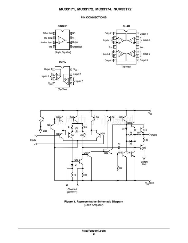
differential inputs and an all NPN transistor output stage.
mode input voltage at ground potential.
exceeded. Specifically, the input voltages must range
maximum rating table. In practice, although
output phase reversal may occur. It is also possible to source
through either inputs鈥?/div>
clamping diode without damage or latching, but phase
reversal may again occur. If at least one input is within the
common mode input voltage range and the other input is
within the maximum input voltage range, no phase reversal
will occur. If both inputs exceed the upper common mode
input voltage limit, the output will be forced to its lowest
voltage state.
Since the input capacitance associated with the small
geometry input device is substantially lower (0.8 pF) than
that of a typical JFET (3.0 pF), the frequency response for
a given input source resistance is greatly enhanced. This
becomes evident in D鈭抰o鈭扐 current to voltage conversion
applications where the feedback resistance can form a pole
with the input capacitance of the op amp. This input pole
creates a 2nd Order system with the single pole op amp and
is therefore detrimental to its settling time. In this context,
lower input capacitance is desirable especially for higher
values of feedback resistances (lower current DACs). This
input pole can be compensated for by creating a feedback
zero with a capacitance across the feedback resistance, if
necessary, to reduce overshoot. For 10 kW of feedback
resistance, the MC33171/72/74 family can typically settle to
within 1/2 LSB of 8 bits in 4.2
ms,
and within 1/2 LSB of 12
bits in 4.8
ms
for a 10 V step. In a standard inverting unity
gain fast settling configuration, the symmetrical slew rate is
typically
卤2.1
V/ms. In the classic noninverting unity gain
configuration the typical output positive slew rate is also
2.1 V/ms, and the corresponding negative slew rate will
usually exceed the positive slew rate as a function of the fall
time of the input waveform.
The all NPN output stage, shown in its basic form on the
equivalent circuit schematic, offers unique advantages over
the more conventional NPN/PNP transistor Class AB output
stage. A 10 kW load resistance can typically swing within
0.8 V of the positive rail (V
CC
) and negative rail (V
EE
),
providing a 28.4 Vpp swing from
卤15
V supplies. This large
output swing becomes most noticeable at lower supply
voltages.
The positive swing is limited by the saturation voltage of
the current source transistor Q7, the V
BE
of the NPN pull鈭抲p
transistor Q17, and the voltage drop associated with the
short circuit resistance, R5. For sink currents less than
0.4 mA, the negative swing is limited by the saturation
voltage of the pull鈭抎own transistor Q15, and the voltage
drop across R4 and R5. For small valued sink currents, the
above voltage drops are negligible, allowing the negative
swing voltage to approach within millivolts of V
EE
. For sink
currents (> 0.4 mA), diode D3 clamps the voltage across R4.
Thus the negative swing is limited by the saturation voltage
of Q15, plus the forward diode drop of D3 (鈮圴
EE
+1.0 V).
Therefore an unprecedented peak鈭抰o鈭抪eak output voltage
swing is possible for a given supply voltage as indicated by
the output swing specifications.
If the load resistance is referenced to V
CC
instead of
ground for single supply applications, the maximum
possible output swing can be achieved for a given supply
voltage. For light load currents, the load resistance will pull
the output to V
CC
during the positive swing and the output
will pull the load resistance near ground during the negative
swing. The load resistance value should be much less than
that of the feedback resistance to maximize pull鈭抲p
capability.
Because the PNP output emitter鈭抐ollower transistor has
been eliminated, the MC33171/72/74 family offers a 15 mA
minimum current sink capability, typically to an output
voltage of (V
EE
+1.8 V). In single supply applications the
output can directly source or sink base current from a
common emitter NPN transistor for current switching
applications.
In addition, the all NPN transistor output stage is
inherently faster than PNP types, contributing to the bipolar
amplifier鈥檚 improved gain bandwidth product. The
associated high frequency low output impedance (200
W
typ
@ 1.0 MHz) allows capacitive drive capability from 0 pF to
400 pF without oscillation in the noninverting unity gain
configuration. The 60掳 phase margin and 15 dB gain margin,
as well as the general gain and phase characteristics, are
virtually independent of the source/sink output swing
conditions. This allows easier system phase compensation,
since output swing will not be a phase consideration. The AC
characteristics of the MC33171/72/74 family also allow
excellent active filter capability, especially for low voltage
single supply applications.
Although the single supply specification is defined at
5.0 V, these amplifiers are functional to at least 3.0 V @
25掳C. However slight changes in parametrics such as
bandwidth, slew rate, and DC gain may occur.
http://onsemi.com
6


 1
1
 2
2
 3
3
 4
4
 5
5
 6
6
 7
7
 8
8
 9
9
 10
10
 11
11
 12
12
 13
13
 14
14
 15
15
 16
16
