MIC5821/5822
Micrel
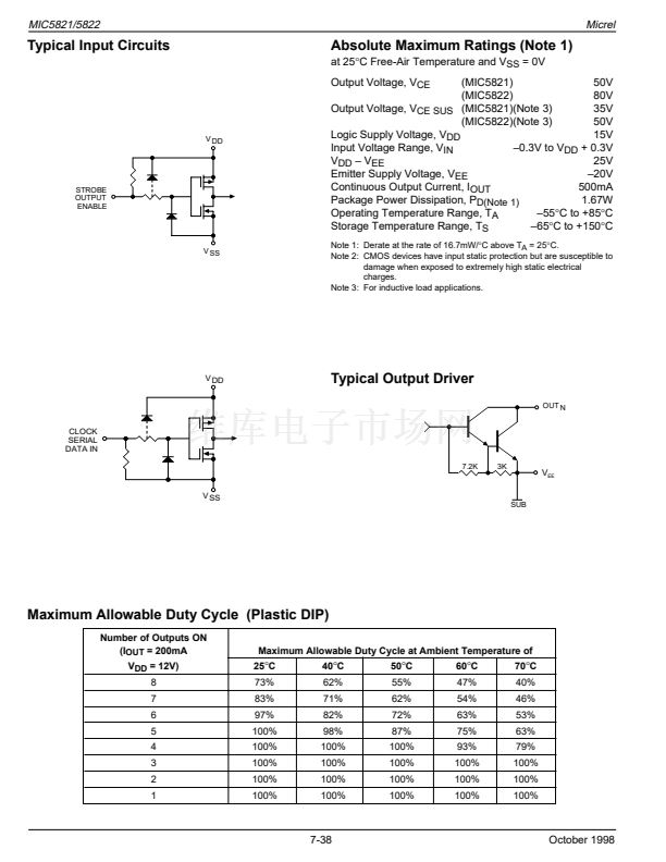
Typical Input Circuits
Absolute Maximum Ratings (Note 1)
at 25掳C Free-Air Temperature and V
SS
= 0V
(MIC5821)
50V
(MIC5822)
80V
Output Voltage, V
CE SUS
(MIC5821)(Note 3)
35V
(MIC5822)(Note 3)
50V
Logic Supply Voltage, V
DD
15V
Input Voltage Range, V
IN
鈥?.3V to V
DD
+ 0.3V
V
DD
鈥?V
EE
25V
Emitter Supply Voltage, V
EE
鈥?0V
Continuous Output Current, I
OUT
500mA
Package Power Dissipation, P
D(Note 1)
1.67W
Operating Temperature Range, T
A
鈥?5掳C to +85掳C
Storage Temperature Range, T
S
鈥?5掳C to +150掳C
Output Voltage, V
CE
Note 1: Derate at the rate of 16.7mW/掳C above T
A
= 25掳C.
Note 2: CMOS devices have input static protection but are susceptible to
damage when exposed to extremely high static electrical
charges.
Note 3: For inductive load applications.
V DD
STROBE
OUTPUT
ENABLE
V SS
V DD
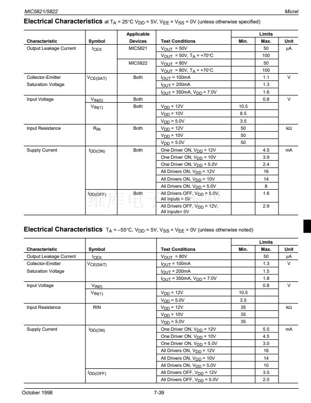
Typical Output Driver
OUT N
CLOCK
SERIAL
DATA IN
7.2K
3K
V
EE
V SS
SUB
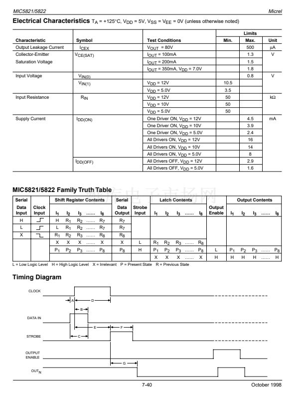
Maximum Allowable Duty Cycle (Plastic DIP)
Number of Outputs ON
(I
OUT
= 200mA
V
DD
= 12V)
8
7
6
5
4
3
2
1
Maximum Allowable Duty Cycle at Ambient Temperature of
25
掳
C
73%
83%
97%
100%
100%
100%
100%
100%
40
掳
C
62%
71%
82%
98%
100%
100%
100%
100%
50
掳
C
55%
62%
72%
87%
100%
100%
100%
100%
60
掳
C
47%
54%
63%
75%
93%
100%
100%
100%
70
掳
C
40%
46%
53%
63%
79%
100%
100%
100%
7-38
October 1998


 1
1
 2
2
 3
3
 4
4
 5
5
