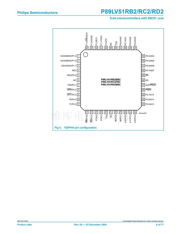
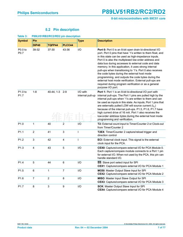
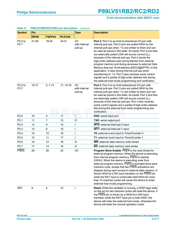
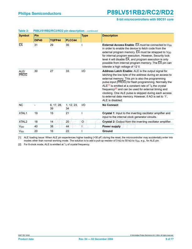
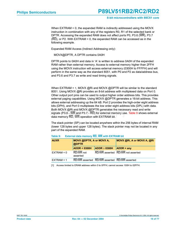
Philips Semiconductors
P89LV51RB2/RC2/RD2
8-bit microcontrollers with 80C51 core
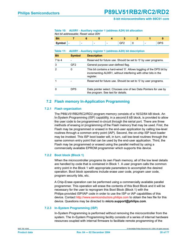
Table 10: AUXR1 - Auxiliary register 1 (address A2H) bit allocation
Not bit addressable; Reset value 00H
Bit
Symbol
Table 11:
Bit
7 to 4
3
2
-
7
-
6
-
5
-
4
3
GF2
0
2
-
1
0
DPS
AUXR1 - Auxiliary register 1 (address A2H) bit description
Symbol
-
GF2
0
Description
Reserved for future use. Should be set to 鈥?鈥?by user programs.
General purpose user-de铿乶ed 铿俛g.
This bit contains a hard-wired 鈥?鈥? Allows toggling of the DPS bit by
incrementing AUXR1, without interfering with other bits in the
register.
Reserved for future use. Should be set to 鈥?鈥?by user programs.
Data pointer select. Chooses one of two Data Pointers for use by
the program. See text for details.
1
0
-
DPS
7.2 Flash memory In-Application Programming
7.2.1
Flash organization
The P89LV51RB2/RC2/RD2 program memory consists of a 16/32/64 kB block. An
In-System Programming (ISP) capability, in a second 8 kB block, is provided to allow
the user code to be programmed in-circuit through the serial port. There are three
methods of erasing or programming of the Flash memory that may be used. First, the
Flash may be programmed or erased in the end-user application by calling low-level
routines through a common entry point (IAP). Second, the on-chip ISP boot loader
may be invoked. This ISP boot loader will, in turn, call low-level routines through the
same common entry point that can be used by the end-user application. Third, the
Flash may be programmed or erased using the parallel method by using a
commercially available EPROM programmer which supports this device.
7.2.2
Boot block (Block 1)
When the microcontroller programs its own Flash memory, all of the low level details
are handled by code that is contained in Block 1. A user program calls the common
entry point in the Block 1 with appropriate parameters to accomplish the desired
operation. Boot block operations include erase user code, program user code,
program security bits, etc.
A Chip-Erase operation can be performed using a commercially available parallel
programmer. This operation will erase the contents of this Boot Block and it will be
necessary for the user to reprogram this Boot Block (Block 1) with the
Philips-provided ISP/IAP code in order to use the ISP or IAP capabilities of this
device. Contact
http://www.semiconductors.philips.com
to obtain the hex 铿乴e for this
device. Questions may be directed to
micro.support@philips.com.
7.2.3
In-System Programming (ISP)
In-System Programming is performed without removing the microcontroller from the
system. The In-System Programming facility consists of a series of internal hardware
resources coupled with internal 铿乺mware to facilitate remote programming of the
9397 750 14342
漏 Koninklijke Philips Electronics N.V. 2004. All rights reserved.
Product data
Rev. 04 鈥?02 December 2004
20 of 77


 1
1
 2
2
 3
3
 4
4
 5
5
 6
6
 7
7
 8
8
 9
9
 10
10
 11
11
 12
12
 13
13
 14
14
 15
15
 16
16
 17
17
 18
18
 19
19
 20
20
 21
21
 22
22
 23
23
 24
24
 25
25
 26
26
 27
27
 28
28
 29
29
 30
30
 31
31
 32
32
 33
33
 34
34
 35
35
 36
36
 37
37
 38
38
 39
39
 40
40
 41
41
 42
42
 43
43
 44
44
 45
45
 46
46
 47
47
 48
48
 49
49
 50
50
 51
51
 52
52
 53
53
 54
54
 55
55
 56
56
 57
57
 58
58
 59
59
 60
60
 61
61
 62
62
 63
63
 64
64
 65
65
 66
66
 67
67
 68
68
 69
69
 70
70
 71
71
 72
72
 73
73
 74
74
 75
75
 76
76
 77
77
