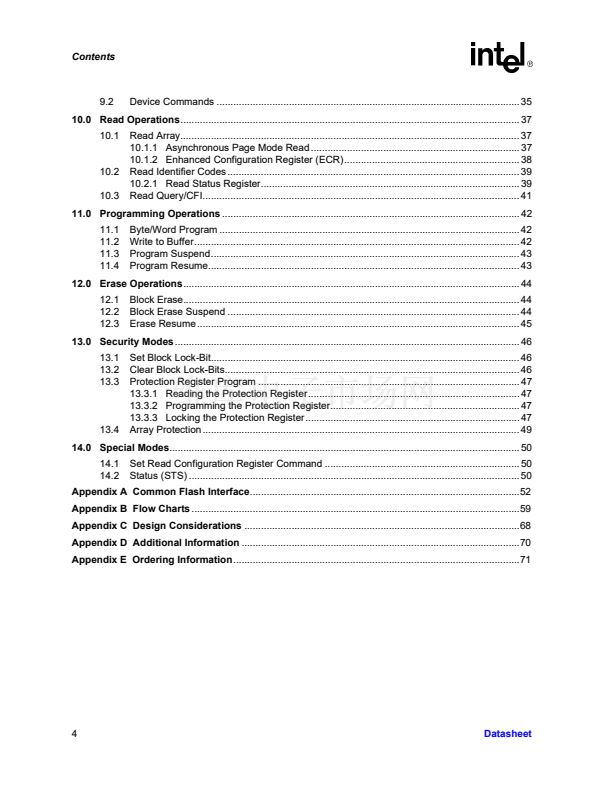
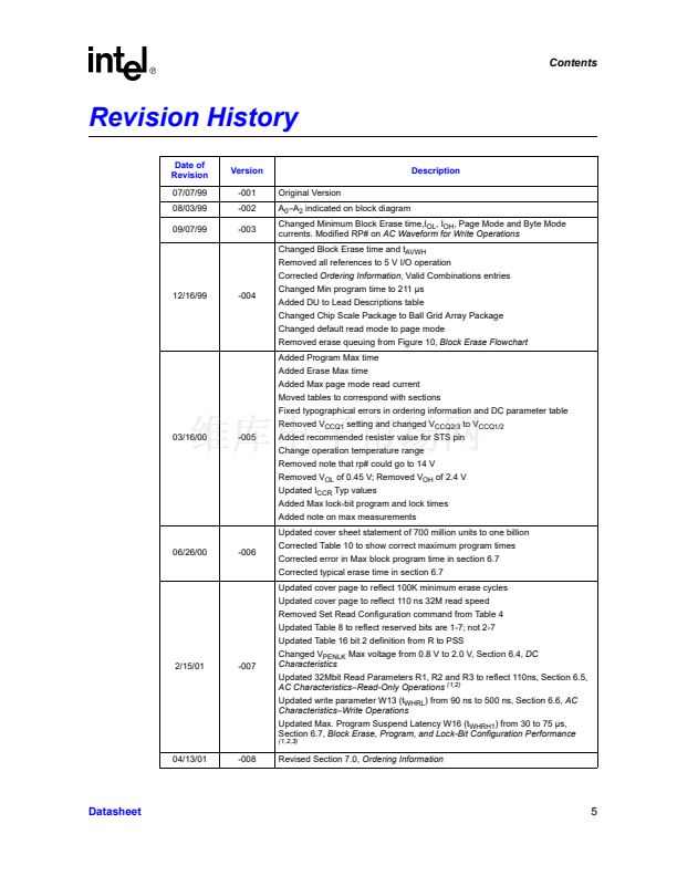
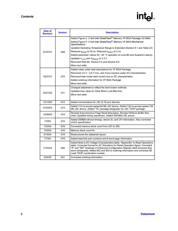
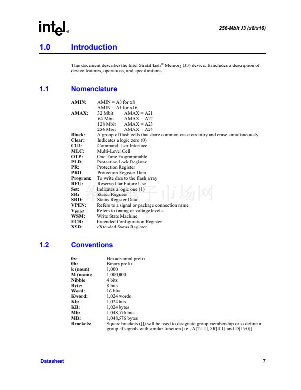
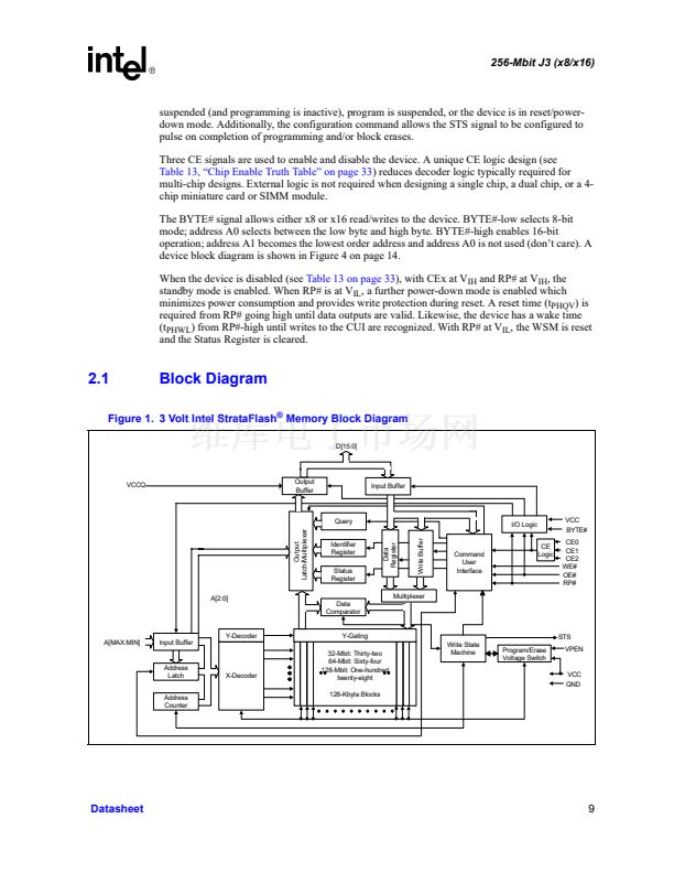
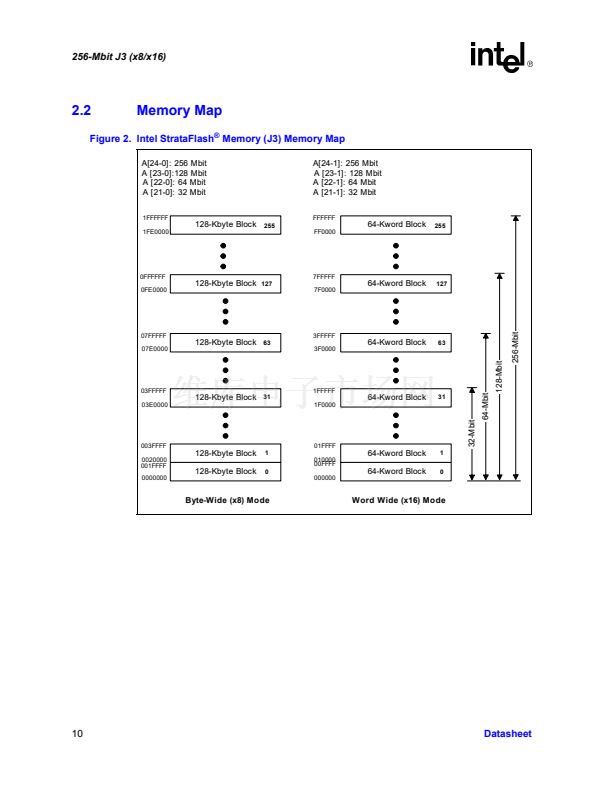
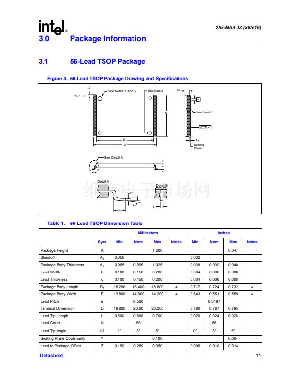
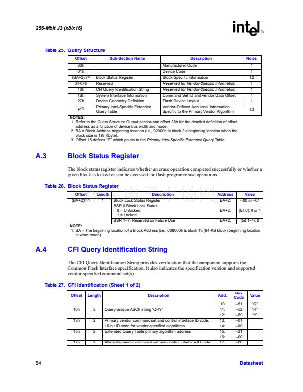
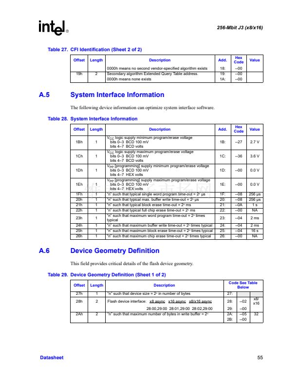
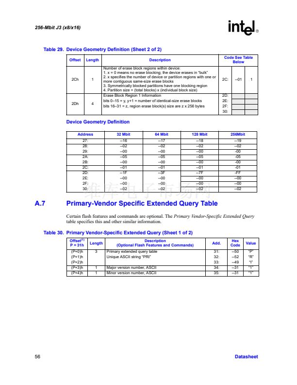
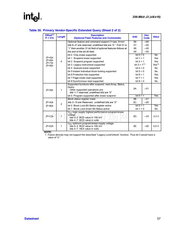
256-Mbit J3 (x8/x16)
7.2
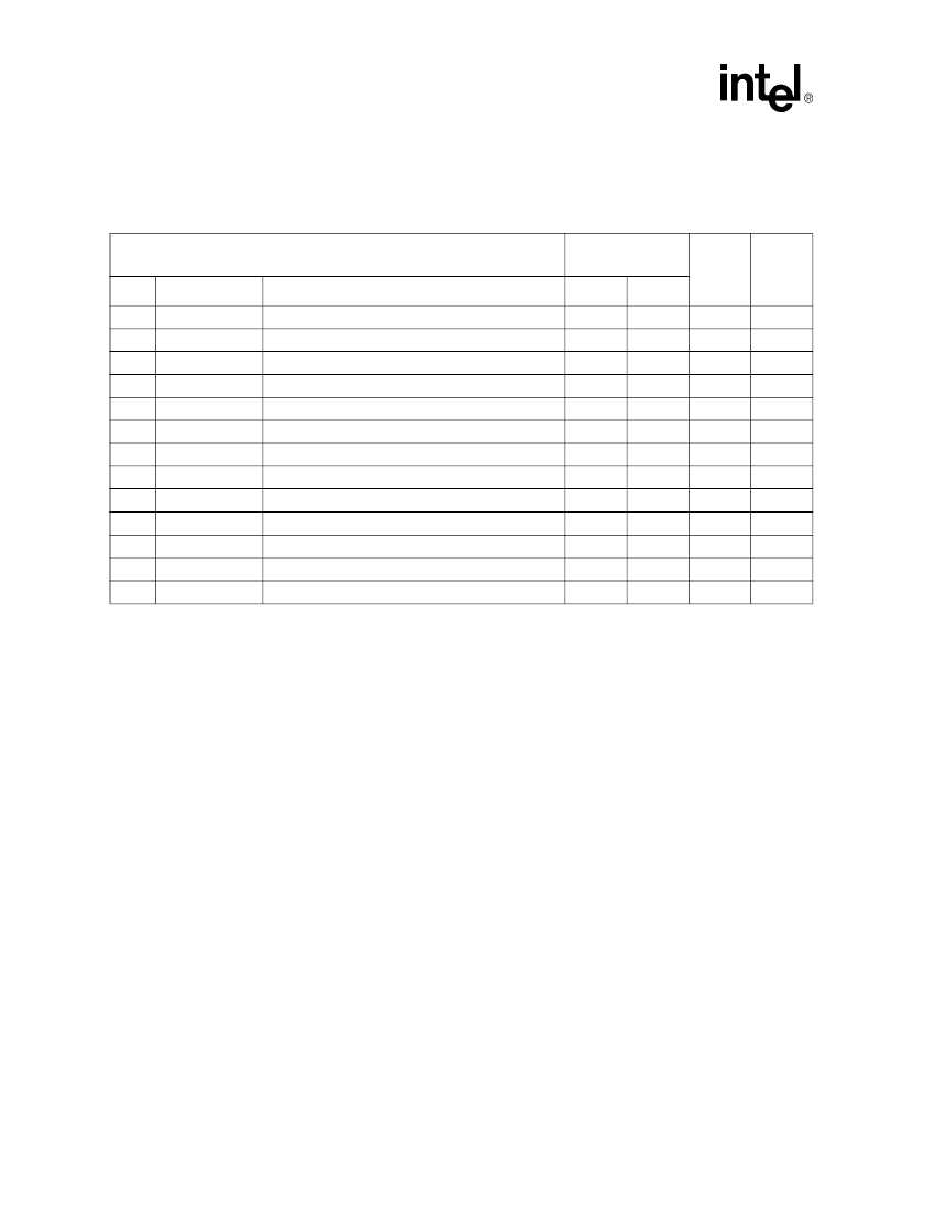
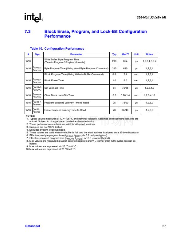
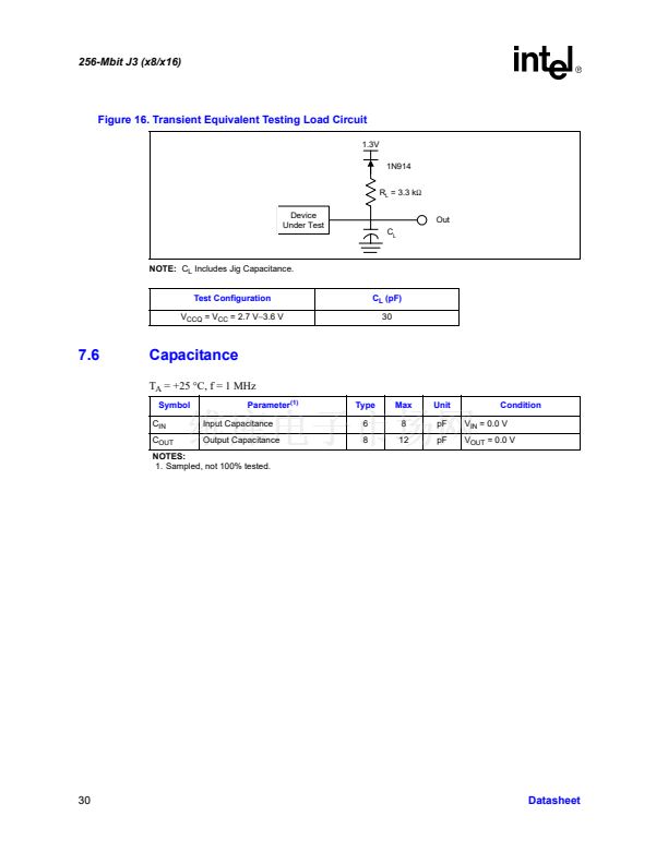
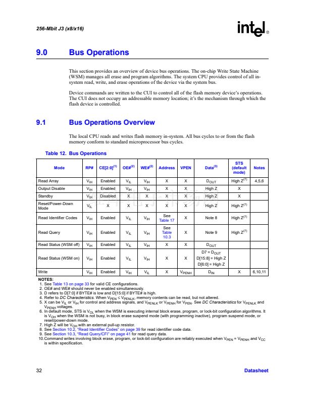
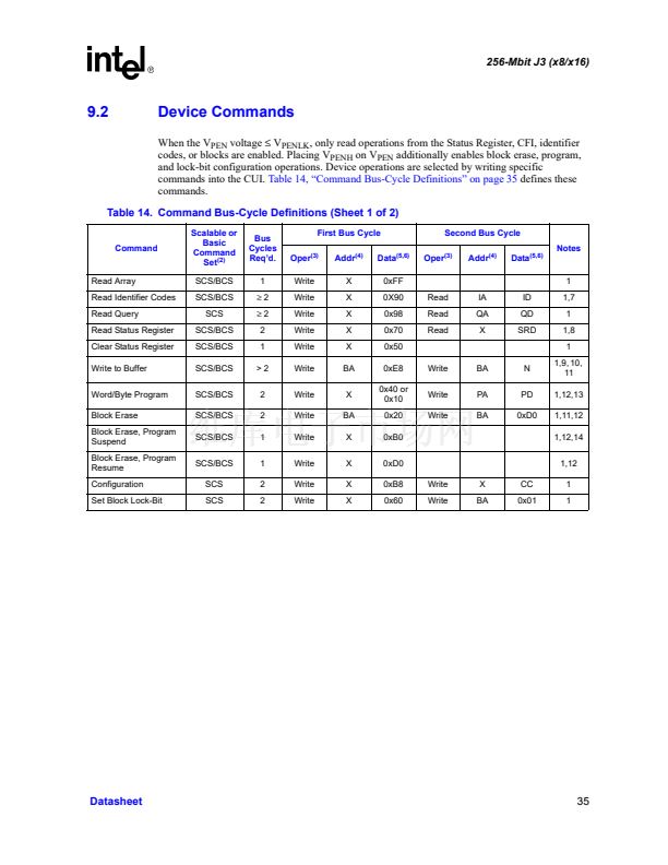
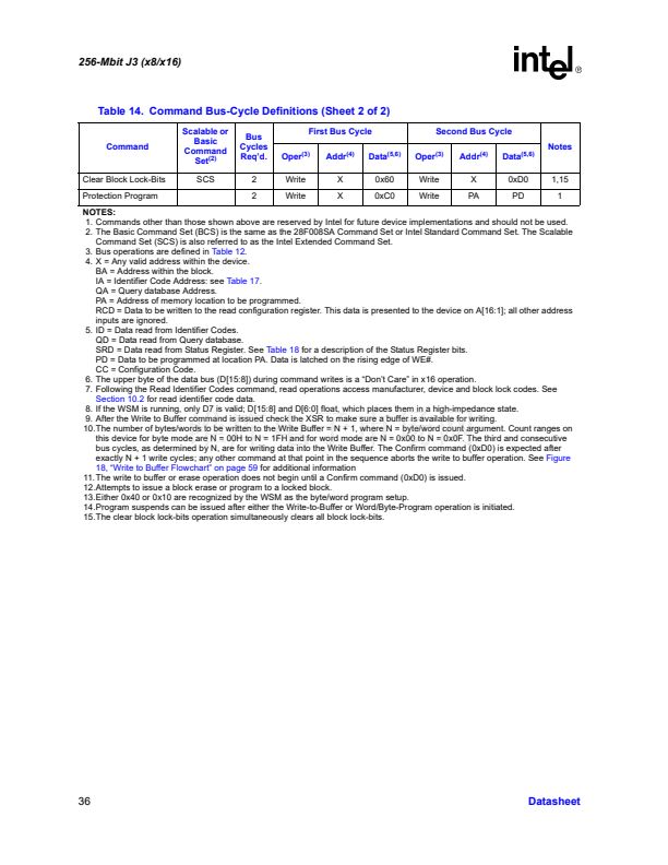
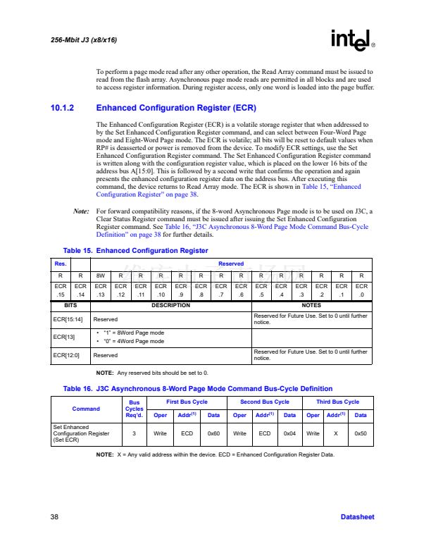
Table 9.
Write Operations
Write Operations
Versions
Valid for All
Speeds
Parameter
RP# High Recovery to WE# (CE
X
) Going Low
CE
X
(WE#) Low to WE# (CE
X
) Going Low
Write Pulse Width
Data Setup to WE# (CE
X
) Going High
Address Setup to WE# (CE
X
) Going High
CE
X
(WE#) Hold from WE# (CE
X
) High
Data Hold from WE# (CE
X
) High
Address Hold from WE# (CE
X
) High
Write Pulse Width High
V
PEN
Setup to WE# (CE
X
) Going High
Write Recovery before Read
WE# (CE
X
) High to STS Going Low
V
PEN
Hold from Valid SRD, STS Going High
0
Min
1
0
70
50
55
0
0
0
30
0
35
500
Max
碌s
ns
ns
ns
ns
ns
ns
ns
ns
ns
ns
ns
ns
1,2,3
1,2,4
1,2,4
1,2,5
1,2,5
1,2,
1,2,
1,2,
1,2,6
1,2,3
1,2,7
1,2,8
1,2,3,8,9
Unit
Notes
#
W1
W2
W3
W4
W5
W6
W7
W8
W9
W11
W12
W13
W15
Symbol
t
PHWL
(t
PHEL
)
t
ELWL
(t
WLEL
)
t
WP
t
DVWH
(t
DVEH
)
t
AVWH
(t
AVEH
)
t
WHEH
(t
EHWH
)
t
WHDX
(t
EHDX
)
t
WHAX
(t
EHAX
)
t
WPH
t
VPWH
(t
VPEH
)
t
WHGL
(t
EHGL
)
t
WHRL
(t
EHRL
)
t
QVVL
NOTES:
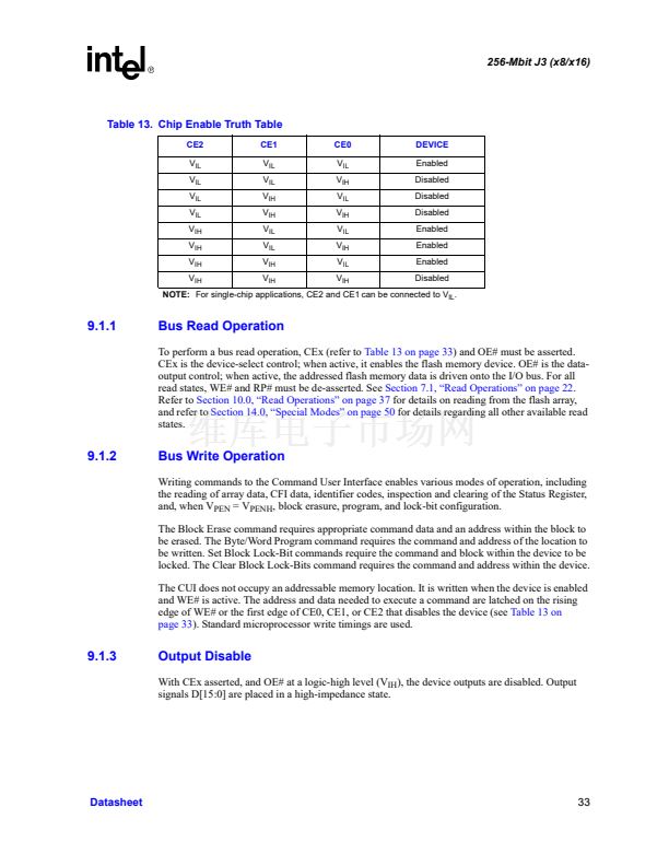
CE
X
low is defined as the first edge of CE0, CE1, or CE2 that enables the device. CE
X
high is defined at the first edge of CE0, CE1,
or CE2 that disables the device (see
Table 13).
1. Read timing characteristics during block erase, program, and lock-bit configuration operations are the same as
during read-only operations. Refer to
AC Characteristics鈥揜ead-Only Operations.
2. A write operation can be initiated and terminated with either CE
X
or WE#.
3. Sampled, not 100% tested.
4. Write pulse width (t
WP
) is defined from CE
X
or WE# going low (whichever goes low last) to CE
X
or WE# going
high (whichever goes high first). Hence, t
WP
= t
WLWH
= t
ELEH
= t
WLEH
= t
ELWH
.
5. Refer to
Table 14
for valid A
IN
and D
IN
for block erase, program, or lock-bit configuration.
6. Write pulse width high (t
WPH
) is defined from CE
X
or WE# going high (whichever goes high first) to CE
X
or WE#
going low (whichever goes low first). Hence, t
WPH
= t
WHWL
= t
EHEL
= t
WHEL
= t
EHWL
.
7. For array access, t
AVQV
is required in addition to t
WHGL
for any accesses after a write.
8. STS timings are based on STS configured in its RY/BY# default mode.
9. V
PEN
should be held at V
PENH
until determination of block erase, program, or lock-bit configuration success
(SR[1,3,4:5] = 0).
26
Datasheet


 1
1
 2
2
 3
3
 4
4
 5
5
 6
6
 7
7
 8
8
 9
9
 10
10
 11
11
 12
12
 13
13
 14
14
 15
15
 16
16
 17
17
 18
18
 19
19
 20
20
 21
21
 22
22
 23
23
 24
24
 25
25
 26
26
 27
27
 28
28
 29
29
 30
30
 31
31
 32
32
 33
33
 34
34
 35
35
 36
36
 37
37
 38
38
 39
39
 40
40
 41
41
 42
42
 43
43
 44
44
 45
45
 46
46
 47
47
 48
48
 49
49
 50
50
 51
51
 52
52
 53
53
 54
54
 55
55
 56
56
 57
57
 58
58
 59
59
 60
60
 61
61
 62
62
 63
63
 64
64
 65
65
 66
66
 67
67
 68
68
 69
69
 70
70
 71
71
 72
72
