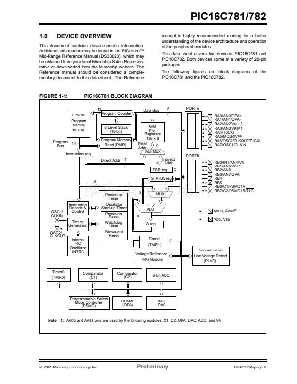
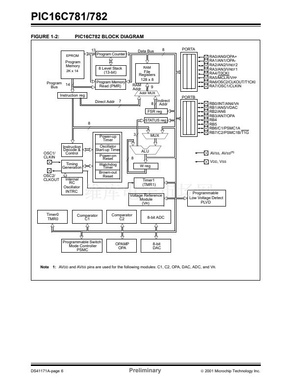
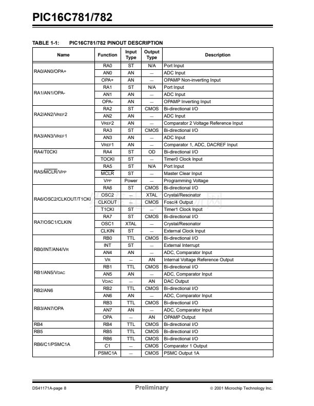
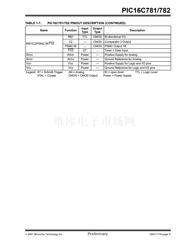
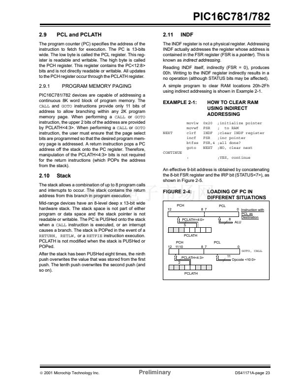
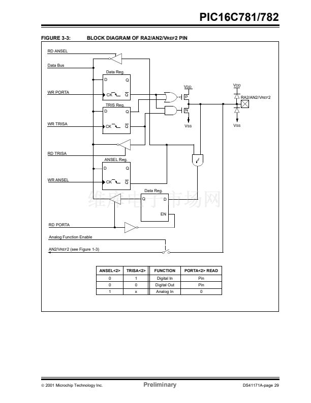
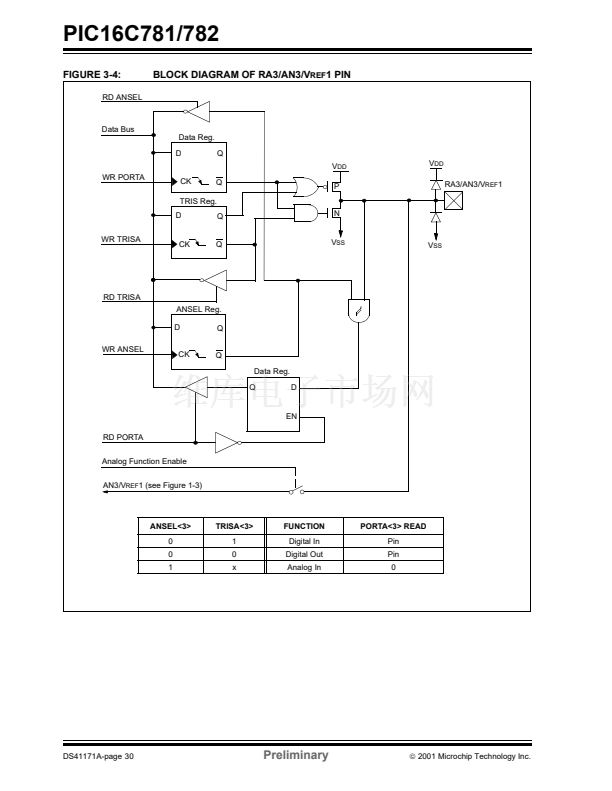
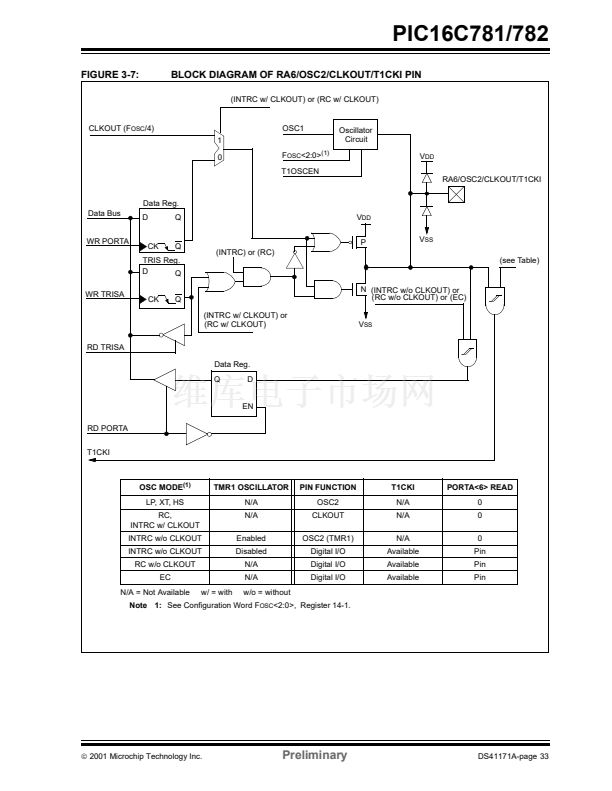
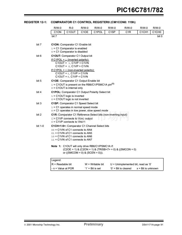
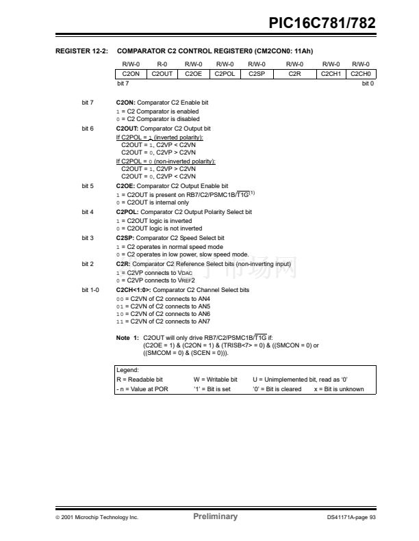
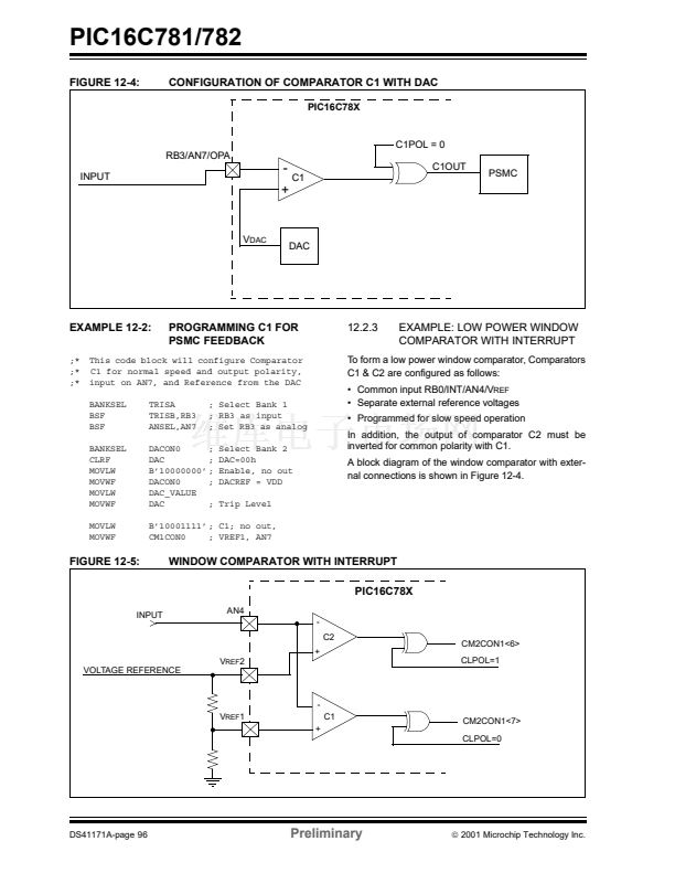
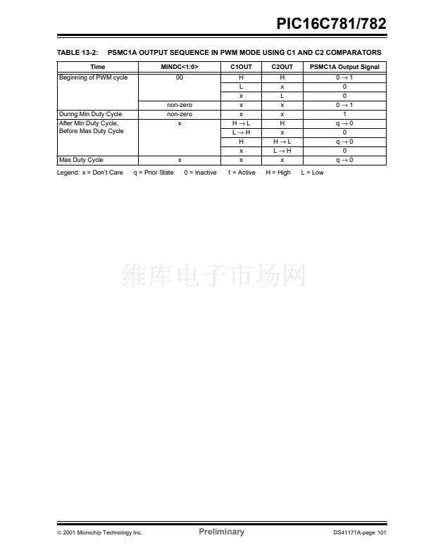
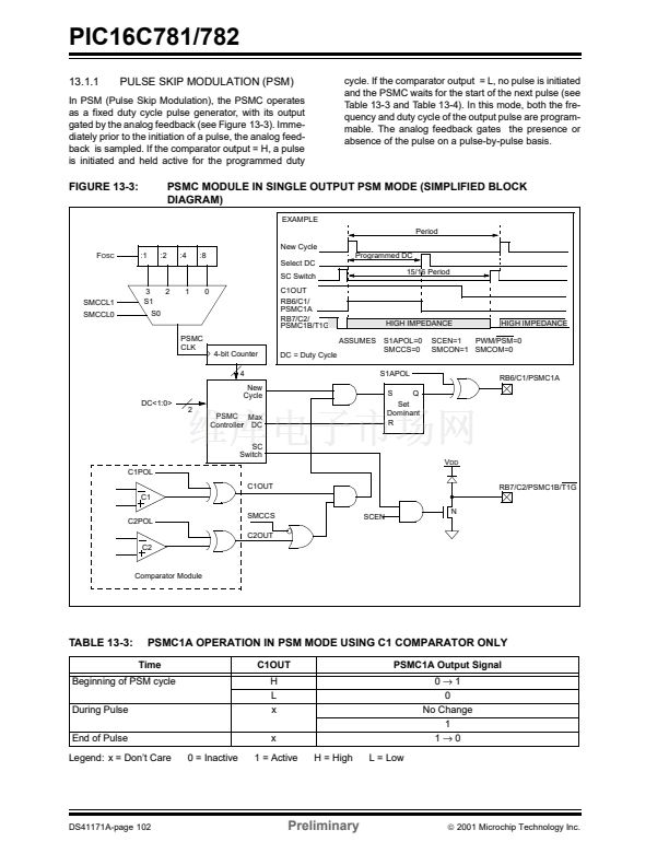
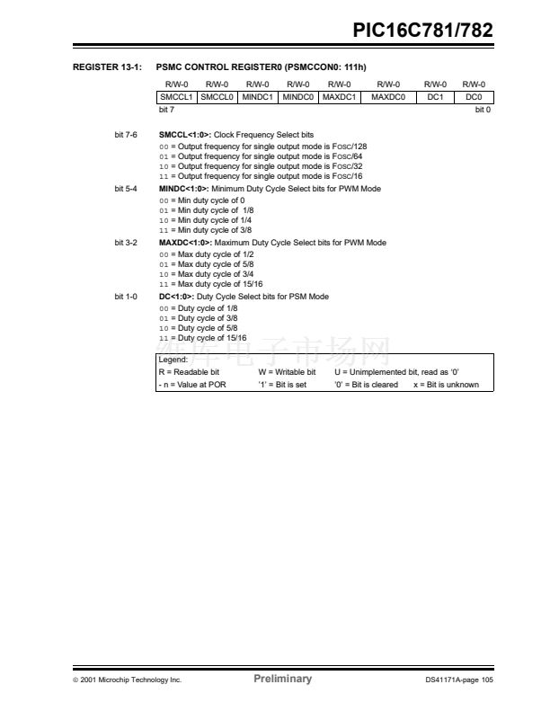
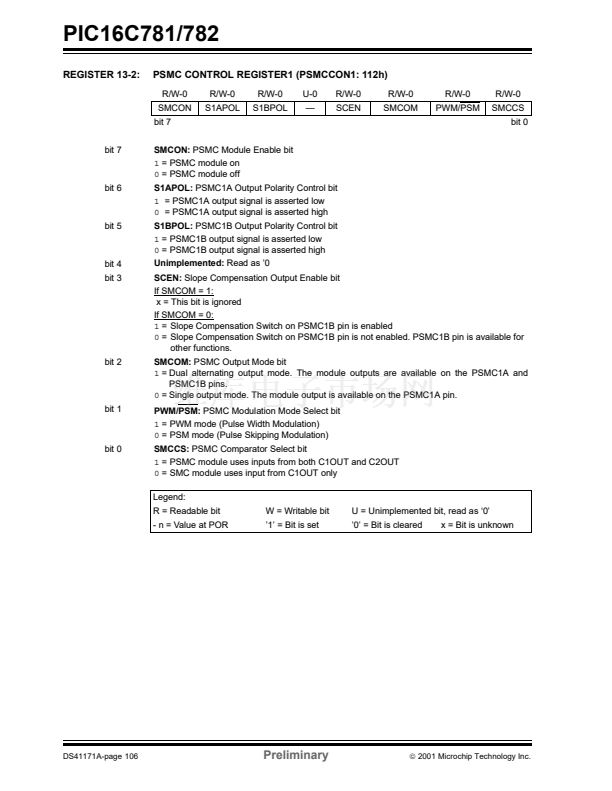
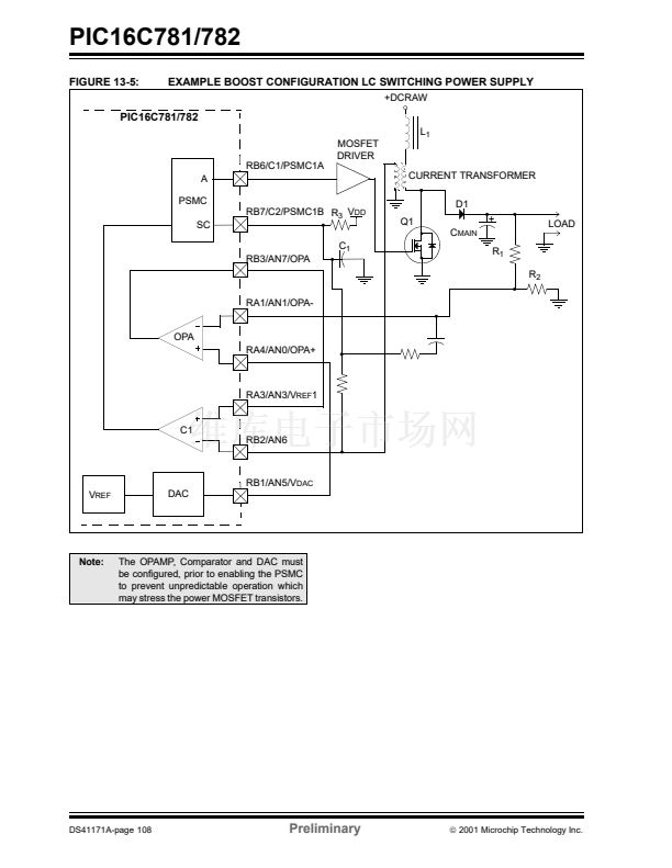
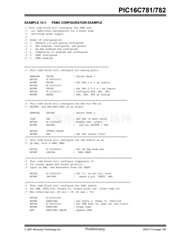
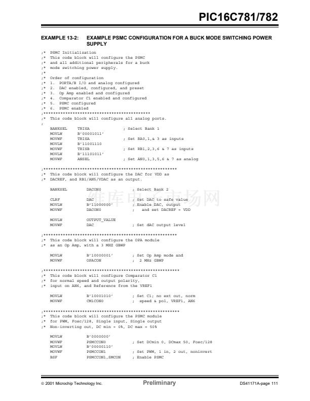
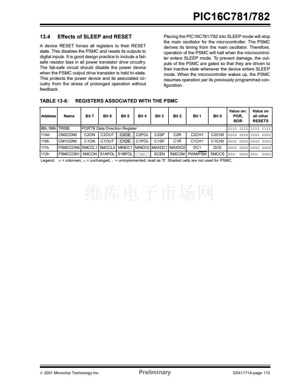
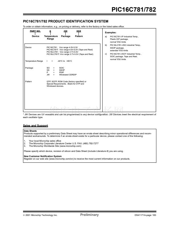
鈥?/div>
The analog positive supply: AV
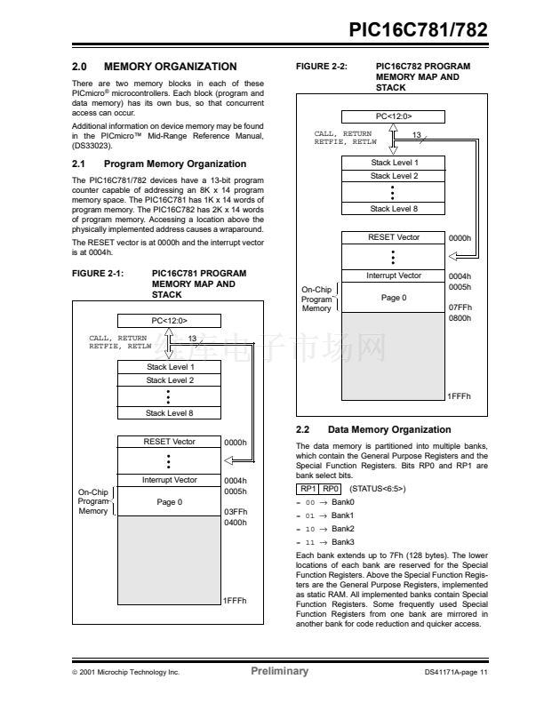
DD
The reference input for Comparator C1: V
REF
1
The Voltage Reference module output: V
R
The DAC Converter module output: V
DAC
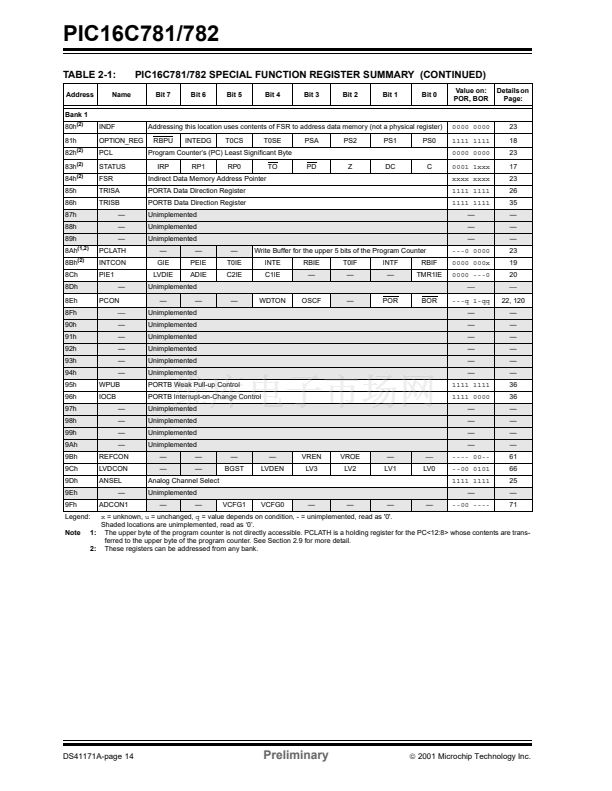
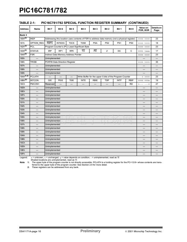
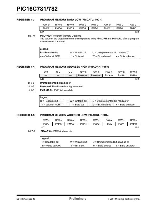
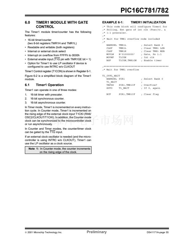
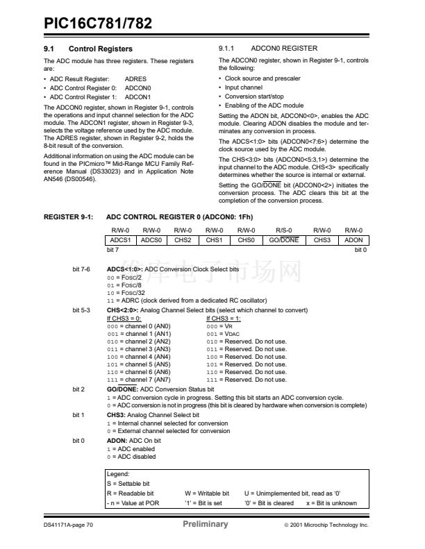
The 8-bit ADC module, shown in Figure 9-1, has 10
inputs in the PIC16C781/782:
鈥?8 external channels, AN<7:0> (RA<3:0> and
RB<3:0>)
鈥?2 internal channels, V
R
and V
DAC
The ADC allows conversion of an analog input signal to
a corresponding 8-bit digital value. The desired chan-
nel is connected to a Sample-and-Hold by the input
multiplexers. The output of the Sample-and-Hold cap-
The ADC has the unique feature of being able to oper-
ate while the device is in SLEEP mode. To operate in
SLEEP, the ADC conversion clock must be derived
from the ADC鈥檚 dedicated internal RC oscillator.
FIGURE 9-1:
ADC MODULE BLOCK DIAGRAM
VOLTAGE COMPARATOR MODULE
OPA MODULE
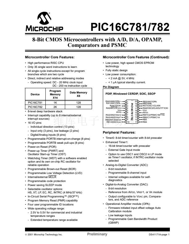
4
RA0/AN0/OPA+
RA1/AN1/OPA-
RA2/AN2/V
REF
2
RA3/AN3/V
REF
1
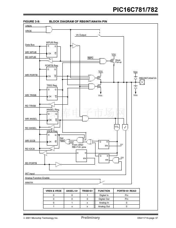
RB0/INT/AN4/V
R
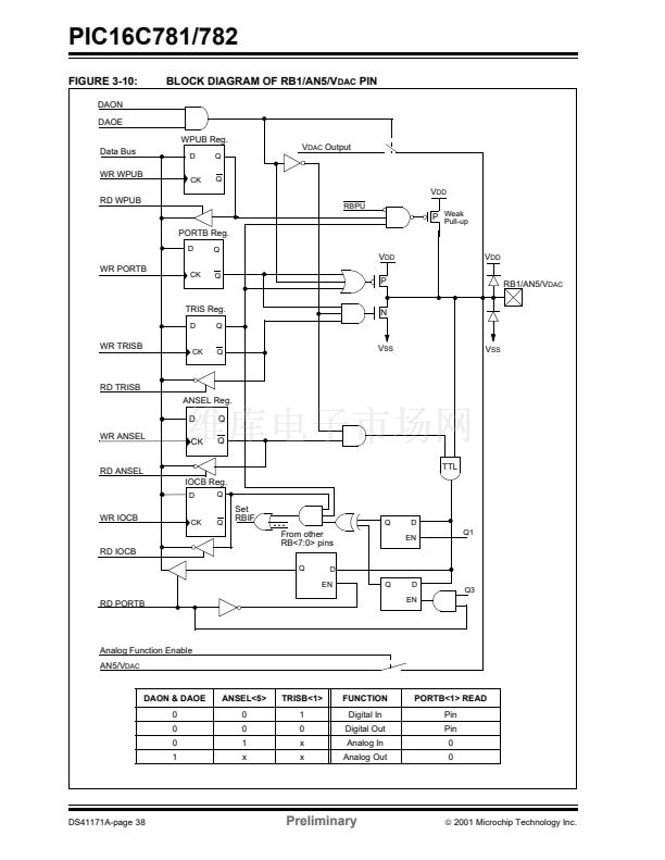
RB1/AN5/V
DAC
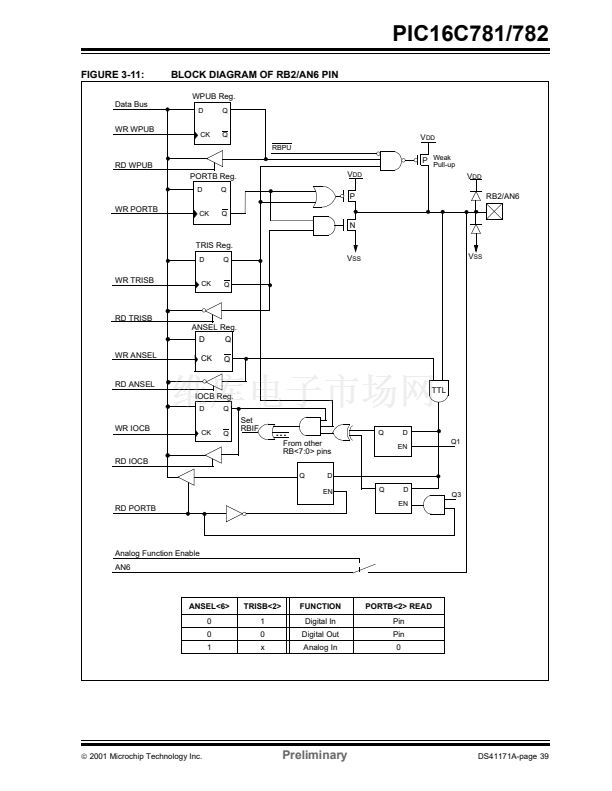
RB2/AN6
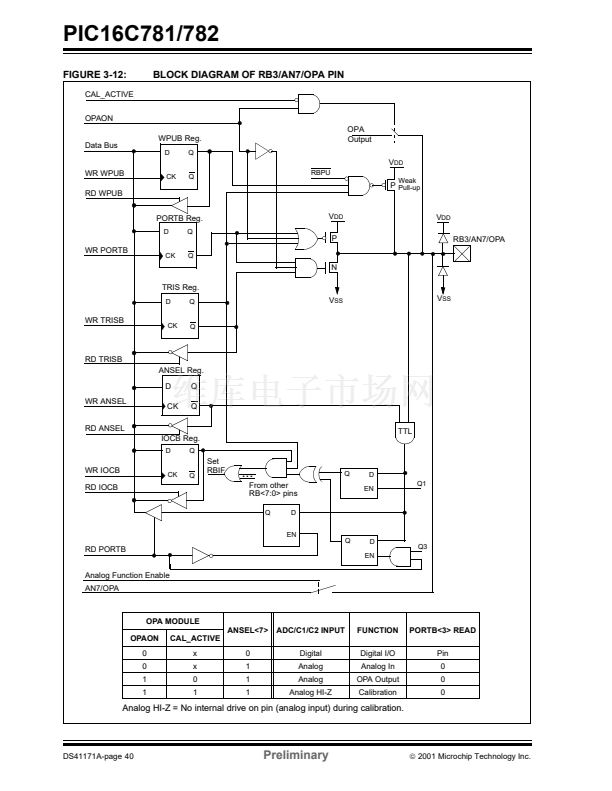
RB3/AN7/OPA
0
1
2
3
4
5
6
7
8
9
DAC MODULE
ADON
GO/DONE
AV
DD
V
REF
1
V
R
V
DAC
0
1
2
3
Sample
and
Hold
ADC
REF
ADC
8
ADRES
CHS<3:0>
VCFG<1:0>
V
R
MODULE
铮?/div>
2001 Microchip Technology Inc.
Preliminary
DS41171A-page 69


 1
1
 2
2
 3
3
 4
4
 5
5
 6
6
 7
7
 8
8
 9
9
 10
10
 11
11
 12
12
 13
13
 14
14
 15
15
 16
16
 17
17
 18
18
 19
19
 20
20
 21
21
 22
22
 23
23
 24
24
 25
25
 26
26
 27
27
 28
28
 29
29
 30
30
 31
31
 32
32
 33
33
 34
34
 35
35
 36
36
 37
37
 38
38
 39
39
 40
40
 41
41
 42
42
 43
43
 44
44
 45
45
 46
46
 47
47
 48
48
 49
49
 50
50
 51
51
 52
52
 53
53
 54
54
 55
55
 56
56
 57
57
 58
58
 59
59
 60
60
 61
61
 62
62
 63
63
 64
64
 65
65
 66
66
 67
67
 68
68
 69
69
 70
70
 71
71
 72
72
 73
73
 74
74
 75
75
 76
76
 77
77
 78
78
 79
79
 80
80
 81
81
 82
82
 83
83
 84
84
 85
85
 86
86
 87
87
 88
88
 89
89
 90
90
 91
91
 92
92
 93
93
 94
94
 95
95
 96
96
 97
97
 98
98
 99
99
 100
100
 101
101
 102
102
 103
103
 104
104
 105
105
 106
106
 107
107
 108
108
 109
109
 110
110
 111
111
 112
112
 113
113
 114
114
 115
115
 116
116
 117
117
 118
118
 119
119
 120
120
 121
121
 122
122
 123
123
 124
124
 125
125
 126
126
 127
127
 128
128
 129
129
 130
130
 131
131
 132
132
 133
133
 134
134
 135
135
 136
136
 137
137
 138
138
 139
139
 140
140
 141
141
 142
142
 143
143
 144
144
 145
145
 146
146
 147
147
 148
148
 149
149
 150
150
 151
151
 152
152
 153
153
 154
154
 155
155
 156
156
 157
157
 158
158
 159
159
 160
160
 161
161
 162
162
 163
163
 164
164
 165
165
 166
166
 167
167
 168
168
 169
169
 170
170
 171
171
 172
172
 173
173
 174
174
 175
175
 176
176
 177
177
 178
178
 179
179
 180
180
 181
181
 182
182
 183
183
 184
184
 185
185
 186
186
