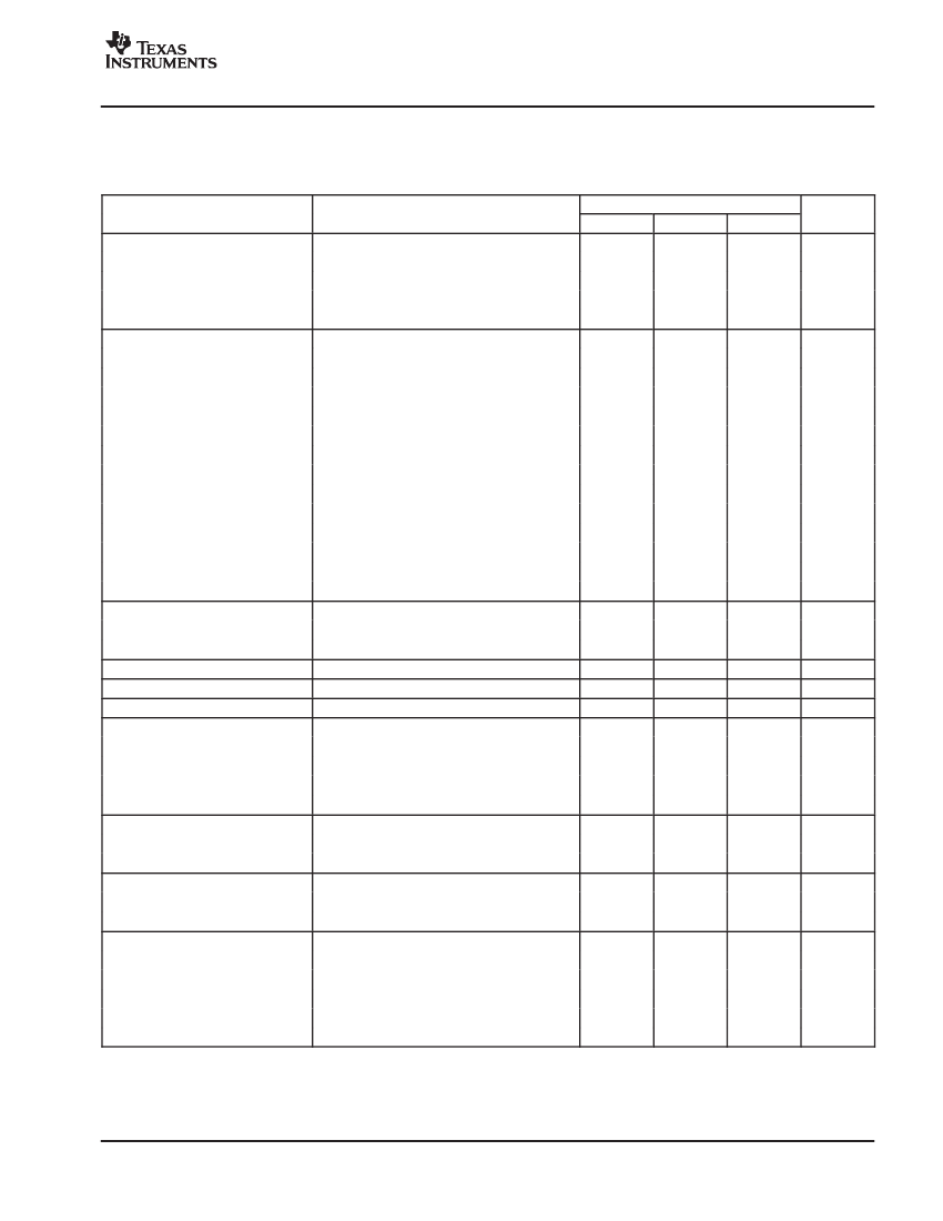
鈮?/div>
5.5V
OUTPUT CURRENT
Nominal
Short Circuit(1)
OSCILLATOR FREQUENCY
(2)
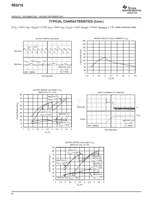
EFFICIENCY
(3)
RIPPLE VOLTAGE
(4)
ENABLE CONTROL
Logic High Input Voltage
Logic Low Input Voltage
Logic High Input Current
Logic Low Input Current
THERMAL SHUTDOWN
Shutdown Temperature
Shutdown Recovery
SUPPLY CURRENT
(Quiescent Current)
In Shutdown Mode
TEMPERATURE RANGE
Specification Ambient Temperature
Operating Ambient Temperature
Storage Ambient Temperature
Thermal Resistance,
q
JA
TA
TA
TA
SOT23鈭?
TSOT23鈭?
鈭?0
鈭?5
鈭?5
200
220
+85
+125
+150
掳C
掳C
掳C
掳C/W
掳C/W
IOUT = 0mA
VIN = 1.8V to 5.5V, Enable = 0V
65
0.01
100
1
碌A
碌A
160
140
掳C
掳C
IOUT = 10mA, VIN = 1.8V, REG710鈭?.3
IOUT = 30mA
VIN = 1.8V to 5.5V
1.3
鈭?.2
VIN
0.4
100
100
V
V
nA
nA
30
100
1.0
90
35
mA
mA
MHz
%
mVp鈭抪
5.2
5.2
4.7
4.7
4.6
3.10
3.10
2.82
2.82
2.54
2.54
2.35
2.35
5.5
5.5
5.0
5.0
5.0
3.3
3.3
3.0
3.0
2.7
2.7
2.5
2.5
5.8
5.8
5.3
5.3
5.4
3.50
3.50
3.18
3.18
2.86
2.86
2.65
2.65
V
V
V
V
V
V
V
V
V
V
V
V
V
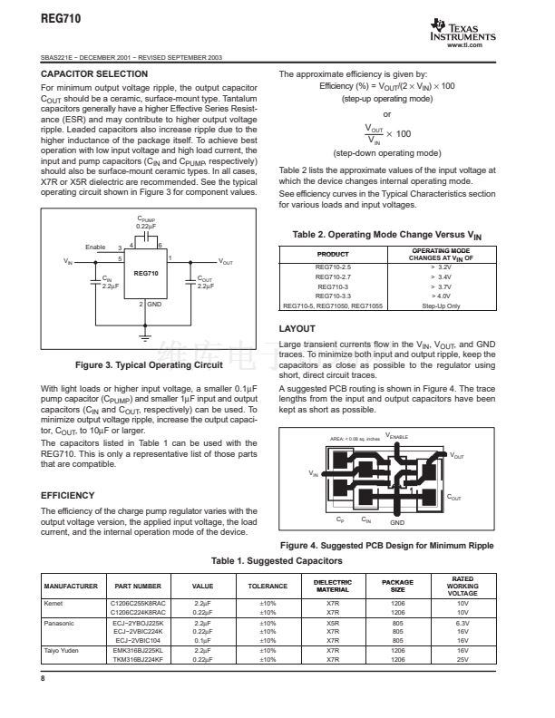
See conditions under Output Voltage
with a resistive load not lower than typical VOUT/IOUT.
3.0
2.7
1.8
5.5
5.5
5.5
V
V
V
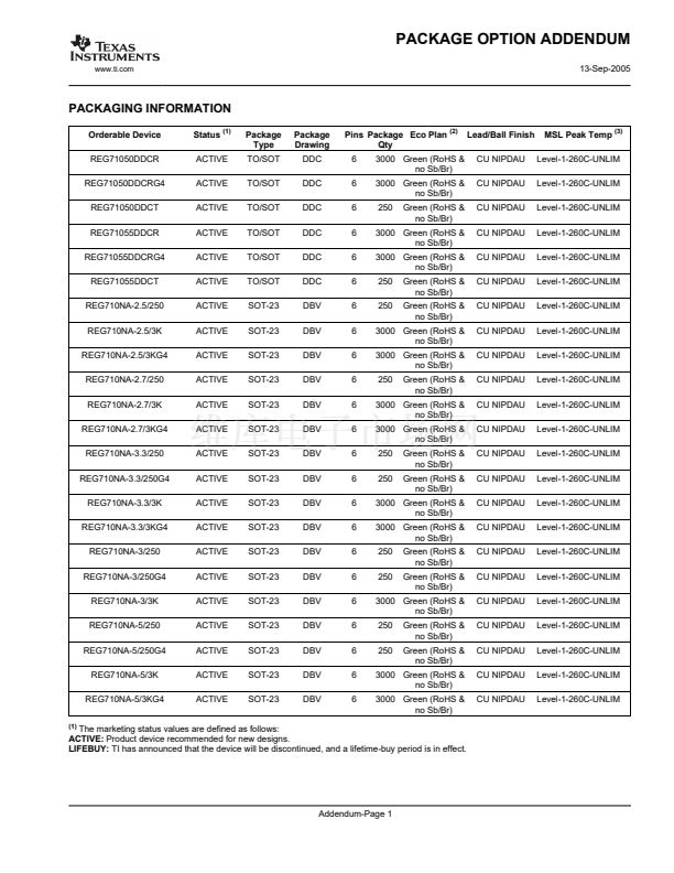
CONDITIONS
MIN
TYP
MAX
UNITS
(1) The supply current is twice the output short-circuit current.
(2) The converter regulates by enabling and disabling periods of switching cycles. The switching frequency is the oscillator frequency during
an active period.
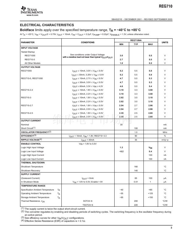
(3) See efficiency curves for other VIN/VOUT configurations.
(4) Effective Series Resistance (ESR) of capacitors is < 0.1鈩?
3


 1
1
 2
2
 3
3
 4
4
 5
5
 6
6
 7
7
 8
8
 9
9
 10
10
 11
11
 12
12
 13
13
 14
14
 15
15
