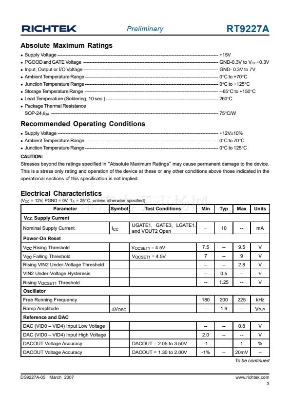
Supply Voltage ---------------------------------------------------------------------------------------------------- +15V
PGOOD and GATE Voltage ------------------------------------------------------------------------------------ GND-0.3V to V
Input, Output or I/O Voltage ------------------------------------------------------------------------------------ GND- 0.3V to 7V
Ambient Temperature Range ----------------------------------------------------------------------------------- 0掳C to +70掳C
Junction Temperature Range ----------------------------------------------------------------------------------- 0掳C to +125掳C
Storage Temperature Range -----------------------------------------------------------------------------------
鈭?/div>
65掳C to +150掳C
Lead Temperature (Soldering, 10 sec.) ---------------------------------------------------------------------- 260掳C
Package Thermal Resistance
SOP-24,胃
JA
-------------------------------------------------------------------------------------------------------- 75掳C/W
Recommended Operating Conditions
Supply Voltage ---------------------------------------------------------------------------------------------------- +12V卤10%
Ambient Temperature Range ----------------------------------------------------------------------------------- 0掳C to 70掳C
Junction Temperature Range ----------------------------------------------------------------------------------- 0掳C to 125掳C
CAUTION:
Stresses beyond the ratings specified in
"Absolute
Maximum Ratings" may cause permanent damage to the device.
This is a stress only rating and operation of the device at these or any other conditions above those indicated in the
operational sections of this specification is not implied.
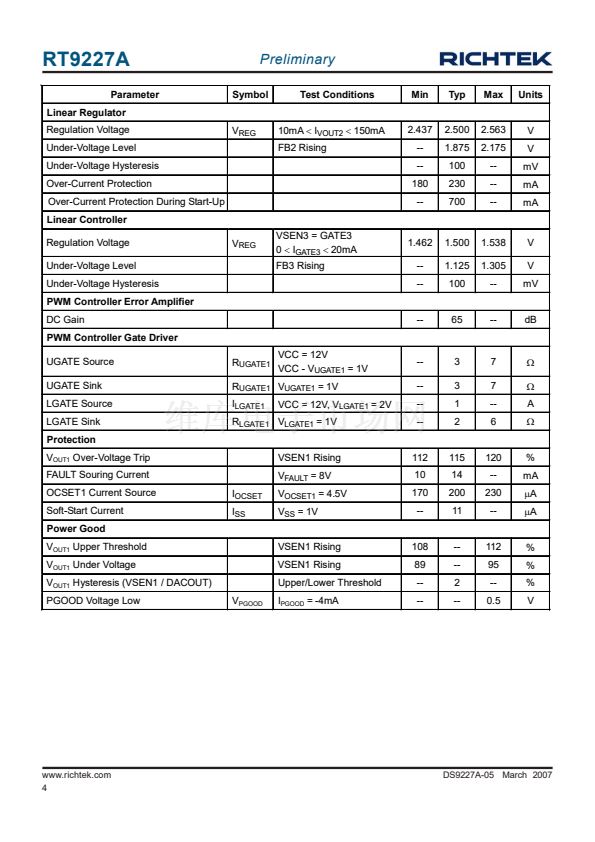
Electrical Characteristics
(V
CC
= 12V, PGND = 0V, T
A
= 25掳C, unless otherwise specified)
Parameter
V
CC
Supply Current
Nominal Supply Current
Power-On Reset
V
CC
Rising Threshold
V
CC
Falling Threshold
Rising VIN2 Under-Voltage Threshold
VIN2 Under-Voltage Hysteresis
Rising V
OCSET1
Threshold
Oscillator
Free Running Frequency
Ramp Amplitude
Reference and DAC
DAC (VID0 鈥?VID4) Input Low Voltage
DAC (VID0 鈥?VID4) Input High Voltage
DACOUT Voltage Accuracy
DACOUT Voltage Accuracy
Symbol
Test Conditions
UGATE1, GATE3, LGATE1,
and VOUT2 Open
V
OCSET1
= 4.5V
V
OCSET1
= 4.5V
Min
Typ
Max
Units
I
CC
--
10
--
mA
7.5
7
--
--
--
--
--
--
0.5
1.25
9.5
9
2.8
--
--
V
V
V
V
V
180
螖V
OSC
--
200
1.9
225
--
kHz
V
P-P
--
2.0
DACOUT = 2.05 to 3.50V
DACOUT = 1.30 to 2.00V
-1
-1%
--
--
--
--
0.8
--
1
20mV
V
V
%
--
To be continued
DS9227A-05 March 2007
www.richtek.com
3


 1
1
 2
2
 3
3
 4
4
 5
5
 6
6
 7
7
 8
8
