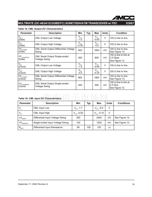
MULTIRATE (OC-48/24/12/3/GBE/FC) SONET/SDH/ATM TRANSCEIVER w/ FEC
Parallel-to-Serial Converter
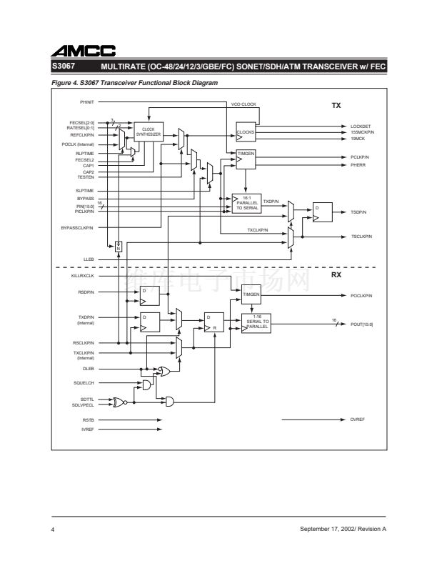
The parallel-to-serial converter shown in Figure 4 is
comprised of a FIFO and a parallel-to-serial register.
The FIFO input latches the data from the PIN[15:0]
bus on the rising edge of PICLK. The parallel-to-
serial register is a loadable shift register which takes
its parallel input from the FIFO output.
An internally generated divide-by-16 clock, which is
phase aligned to the transmit serial clock as de-
scribed in the
Timing Generator
description, activates
the parallel data transfer between registers. The serial
data is shifted out of the parallel-to-serial register at
the TSCLK rate.
S3067
FIFO
A FIFO is added to decouple the internal and exter-
nal (PICLK) clocks. The internally generated
divide-by-16 clock is used to clock out data from the
FIFO. PHINIT and LOCKDET are used to center or
reset the FIFO. The PHINIT and LOCKDET signals
will center the FIFO after the third PICLK pulse. This
is to insure that PICLK is stable. This scheme allows
the user to have an infinite PCLK-to-PICLK delay
through the ASIC. Once the FIFO is centered, the
PCLK-to-PICLK delay can have a maximum drift as
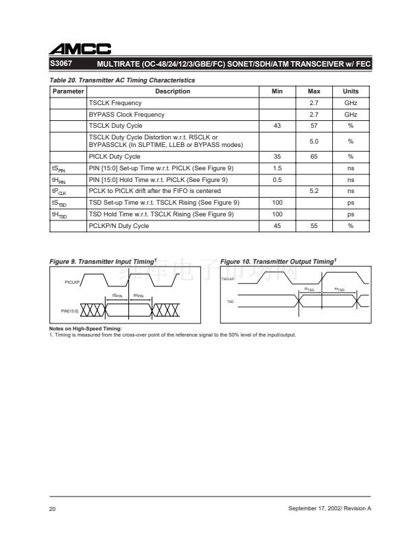
specified in Table 20.
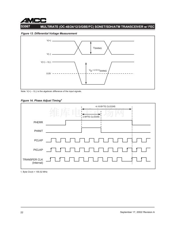
internally generated clock is the same, their phase
relationship is arbitrary. To prevent errors caused by
short setup or hold times between the two timing
domains, the timing generator circuitry monitors the
phase relationship between PICLK and the internally
generated clock. When a potential setup or hold time
violation is detected, the phase error goes high.
When PHERR conditions occur, PHINIT should be
activated to recenter the FIFO (at least 2 PCLK peri-
ods). This can be done by connecting PHERR to
PHINIT. When realignment occurs, up to 10 bytes of
data will be lost. The user can also take in the
PHERR signal, process it and send an output to
PHINIT in such a way that idle bytes are lost during
the realignment process. PHERR will go inactive
when the realignment is complete.
Receiver Operation
The S3067 receiver chip provides the first stage of
digital processing of a receive SONET STS-48/STS-
24/STS-12/STS-3/GBE/FC bit-serial stream. The
bit-serial data stream is then converted into a 16-bit
half-word data format. A loopback mode is provided
for diagnostic loopback (transmitter to receiver). A line
loopback (receiver to transmitter) is also provided.
Both line and local loopback modes can be active at
the same time.
FIFO Initialization
The FIFO can be initialized in one of the following
three ways:
1. During power up, once the PLL has locked to
the reference clock provided on the REFCLK
pins, the LOCKDET will go active and initialize
the FIFO.
2. When RSTB goes active, the entire chip is reset.
This causes the PLL to go out of lock and thus
the LOCKDET goes inactive. When the PLL re-
acquires the lock, the LOCKDET goes active
and initializes the FIFO. Note: PCLK is held re-
set when RSTB is active.
3. The user can also initialize the FIFO by raising
PHINIT.
During the normal running operation, the incoming
data is passed from the PICLK timing domain to the
internally generated, divide-by-16 clock timing do-
main. Although the frequency of PICLK and the
Serial-to-Parallel Converter
The serial-to-parallel converter consists of two 16-bit
registers. The first is a serial-in, parallel-out shift reg-
ister, which performs the serial-to-parallel conversion
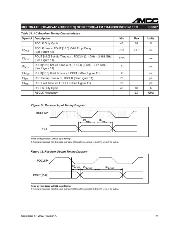
clocked by the clock recovery block. On the falling
edge of the POCLK, the data in the parallel register
is transferred to an output parallel register which
drives POUT[15:0].
OTHER OPERATING MODES
Diagnostic Loopback
When the Diagnostic Loopback Enable (DLEB) input
is low, a loopback from the transmitter to the re-
ceiver at the serial data rate can be set up for
diagnostic purposes. The differential serial output
data from the transmitter is routed to the serial-to-
parallel block in place of the normal data stream
(RSD). TSD/TSCLK outputs are active. DLEB takes
precedence over SDPECL and SDTTL.
September 17, 2002/ Revision A
7


 1
1
 2
2
 3
3
 4
4
 5
5
 6
6
 7
7
 8
8
 9
9
 10
10
 11
11
 12
12
 13
13
 14
14
 15
15
 16
16
 17
17
 18
18
 19
19
 20
20
 21
21
 22
22
 23
23
 24
24
 25
25
 26
26
 27
27
