Si91872
Vishay Siliconix
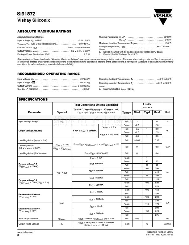
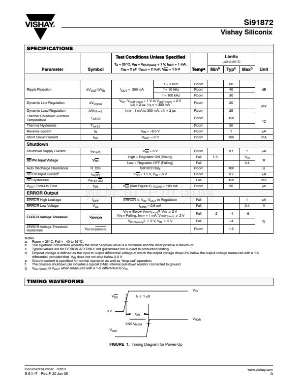
SPECIFICATIONS
Test Conditions Unless Specified
Parameter
Symbol
T
A
= 25_C, V
IN
= V
OUT(nom)
+ 1 V, I
OUT
= 1 mA,
C
IN
= 2
mF,
C
OUT
= 2.0
mF,
V
SD
= 1.5 V
Limits
鈭?0
to 85_C
Temp
a
Room
Room
Room
Room
Room
Room
Room
Min
b
Typ
c
60
40
30
20
25
150
20
1
700
Max
b
Unit
f = 1 kHz
Ripple Rejection
pp
j
DV
OUT
/DV
IN
DV
O(line)
DV
O(load)
T
J(S/D)
T
HYST
I
R
I
SC
V
IN
=
鈭?.0
V
V
OUT
= 0 V
I
OUT
= 300 mA
f = 10 kHz
f = 100 kHz
Dynamic Line Regulation
Dynamic Load Regulation
Thermal Shutdown Junction
Temperature
Thermal Hysteresis
Reverse current
Short Circuit Current
V
IN
: V
OUT(nom)
+ 1 V to V
OUT(nom)
+ 2 V
t
r
/t
f
= 2
ms,
I
OUT
= 300 mA
I
OUT
: 1 mA to 300 mA, t
r
/t
f
= 2
ms
dB
mV
_C
C
mA
mA
Room
Room
Shutdown
Shutdown Supply Current
SD Pin Input Voltage
Auto Discharge Resistance
SD Pin Input Current
f
SD Hysteresis
V
OUT
Turn-On Time
I
CC(off)
V
SD
R_DIS
I
IN(SD)
V
HYST(SD)
t
ON
V
SD
(See Figure 1), I
LOAD
= 100 mA
V
SD
= 0 V
High = Regulator ON (Rising)
Low = Regulator OFF (Falling)
Si91872 Only
V
SD
= 1.5 V, V
IN
= 6 V
Room
Full
Full
Room
Room
Full
Room
100
0.7
150
50
1.5
0.1
1
V
IN
0.4
mA
V
W
mA
mV
ms
ERROR Output
ERROR High Leakage
ERROR Low Voltage
ERROR Voltage Threshold
ERROR Voltage Threshold
Hysteresis
I
OFF
V
OL
V
ERROR
V
HYST(ERROR)
ERROR
v
V
IN
. V
OUT
in Regulation
I
SINK
= 0.5 mA
V
OUT
Below V
OUT(nom)g
, V
IN
w
2 V
V
OUT
Falling, I
OUT
= 1 mA, V
OUT(nom)
w
2 V
V
OUT(nom)g
t
2 V, V
IN
u
2 V
Full
Full
Full
Full
Room
鈭?
鈭?
鈭?
1.5
1
0.4
鈭?
%
mA
V
Notes
a. Room = 25_C, Full =
鈭?0
to 85_C.
b. The algebraic convention whereby the most negative value is a minimum and the most positive a maximum.
c. Typical values are for DESIGN AID ONLY, not guaranteed nor subject to production testing.
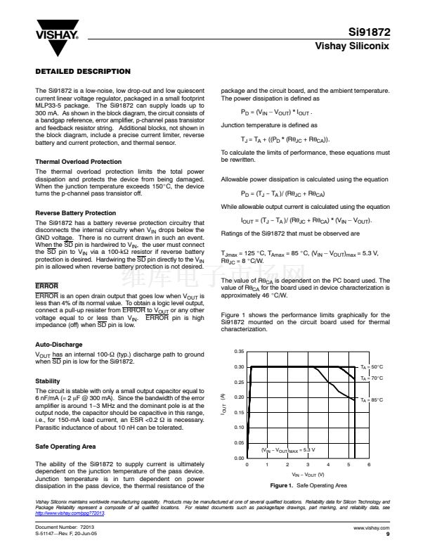
d. Dropout voltage is defined as the input to output differential voltage at which the output voltage drops 2% below the output voltage measured with a 1-V
differential, provided that V
IN
does not not drop below 2.0 V.
e. Ground current is specified for normal operation as well as 鈥渄rop-out鈥?operation.
f.
The device鈥檚 shutdown pin includes a typical 2-MW internal pull-down resistor connected to ground.
g. V
OUT(nom)
is V
OUT
when measured with a 1-V differential to V
IN
.
TIMING WAVEFORMS
V
IN
V
SD
t
r
v
1
mS
0V
t
ON
V
NOM
0.95 V
NOM
V
OUT
FIGURE 1.
Timing Diagram for Power-Up
Document Number: 72013
S-51147鈥擱ev. F, 20-Jun-05
www.vishay.com
3


 1
1
 2
2
 3
3
 4
4
 5
5
 6
6
 7
7
 8
8
 9
9
