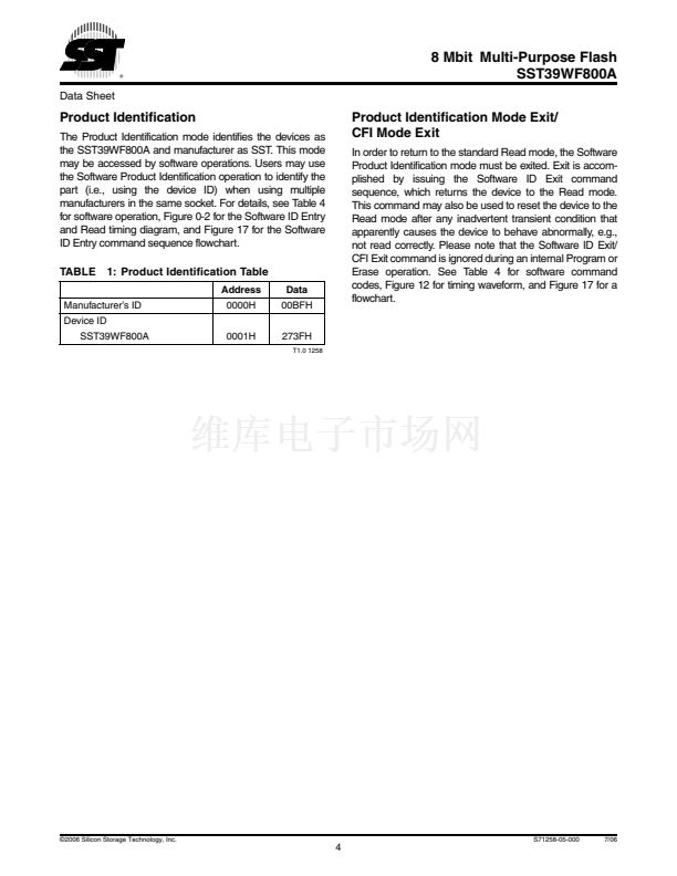
8 Mbit Multi-Purpose Flash
SST39WF800A
Data Sheet
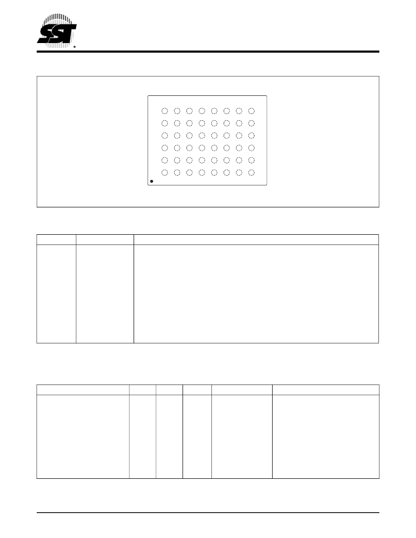
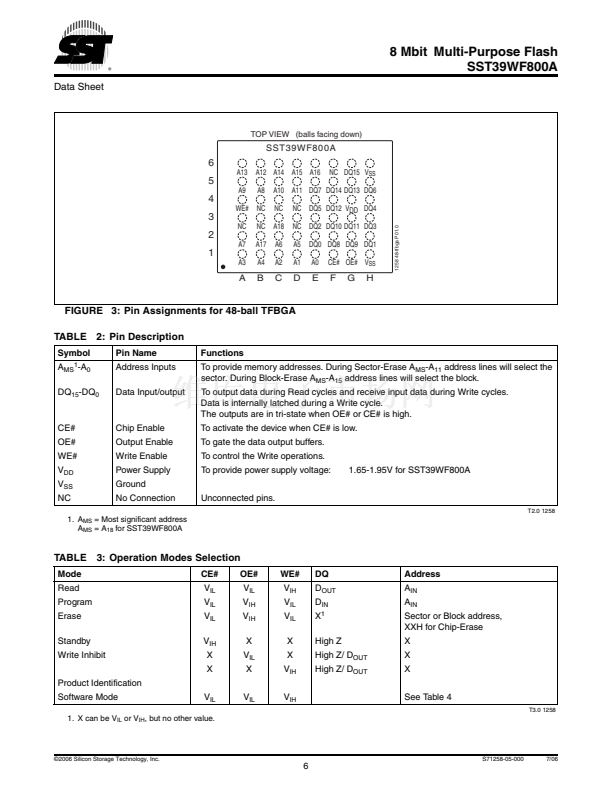
TOP VIEW (balls facing down)
SST39WF800A
6
A13
A12 A14 A15 A16
A8
NC
NC
A17
A4
5
A9
NC DQ15 V
SS
A10 A11 DQ7 DQ14 DQ13 DQ6
NC
A18
A6
A2
NC DQ5 DQ12 VDD DQ4
1258 48-tfbga P01.0
4
WE#
3
NC
NC DQ2 DQ10 DQ11 DQ3
A5
A1
DQ0 DQ8 DQ9 DQ1
A0
CE# OE# V
SS
2
A7
1
A3
A
B
C
D
E
F
G
H
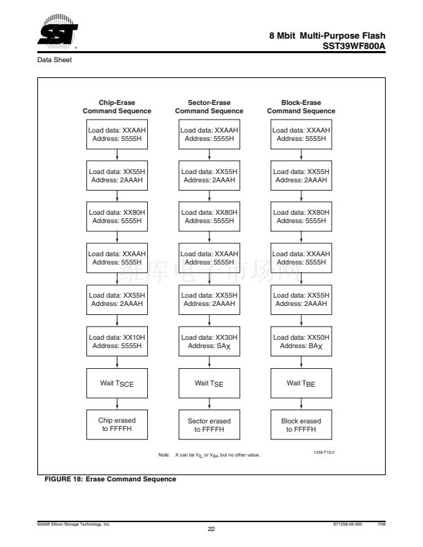
FIGURE 3: Pin Assignments for 48-ball TFBGA
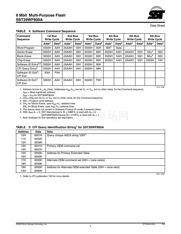
TABLE 2: Pin Description
Symbol
A
MS1
-A
0
DQ
15
-DQ
0
Pin Name
Address Inputs
Data Input/output
Functions
To provide memory addresses. During Sector-Erase A
MS
-A
11
address lines will select the
sector. During Block-Erase A
MS
-A
15
address lines will select the block.
To output data during Read cycles and receive input data during Write cycles.
Data is internally latched during a Write cycle.
The outputs are in tri-state when OE# or CE# is high.
To activate the device when CE# is low.
To gate the data output buffers.
To control the Write operations.
To provide power supply voltage:
Unconnected pins.
T2.0 1258
CE#
OE#
WE#
V
DD
V
SS
NC
Chip Enable
Output Enable
Write Enable
Power Supply
Ground
No Connection
1.65-1.95V for SST39WF800A
1. A
MS
= Most significant address
A
MS
= A
18
for SST39WF800A
TABLE 3: Operation Modes Selection
Mode
Read
Program
Erase
Standby
Write Inhibit
Product Identification
Software Mode
V
IL
V
IL
V
IH
See Table 4
T3.0 1258
CE#
V
IL
V
IL
V
IL
V
IH
X
X
OE#
V
IL
V
IH
V
IH
X
V
IL
X
WE#
V
IH
V
IL
V
IL
X
X
V
IH
DQ
D
OUT
D
IN
X
1
High Z
High Z/ D
OUT
High Z/ D
OUT
Address
A
IN
A
IN
Sector or Block address,
XXH for Chip-Erase
X
X
X
1. X can be V
IL
or V
IH
, but no other value.
漏2006 Silicon Storage Technology, Inc.
S71258-05-000
7/06
6


 1
1
 2
2
 3
3
 4
4
 5
5
 6
6
 7
7
 8
8
 9
9
 10
10
 11
11
 12
12
 13
13
 14
14
 15
15
 16
16
 17
17
 18
18
 19
19
 20
20
 21
21
 22
22
 23
23
 24
24
 25
25
