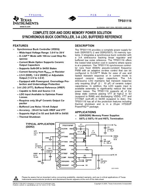
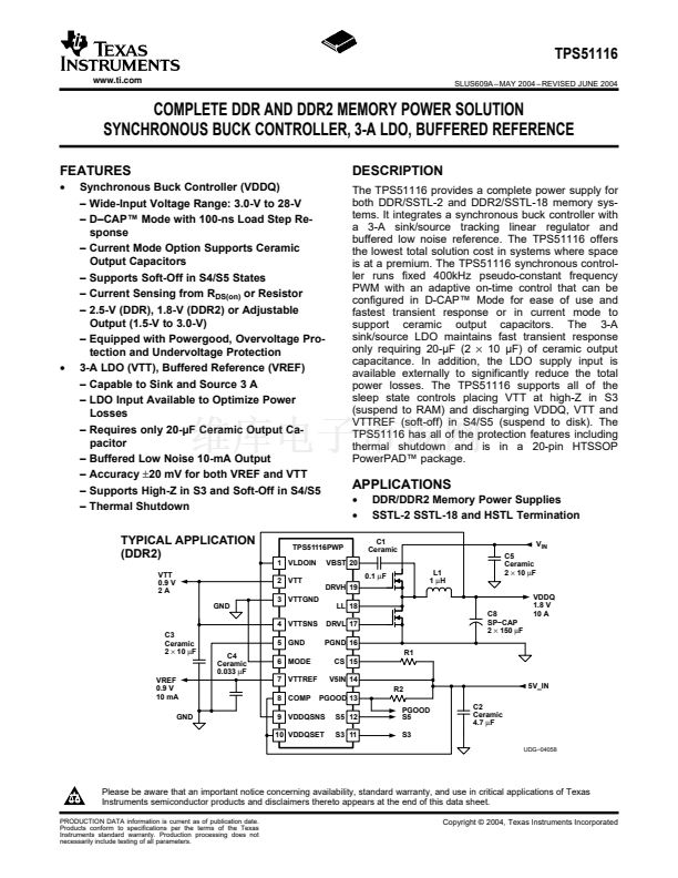
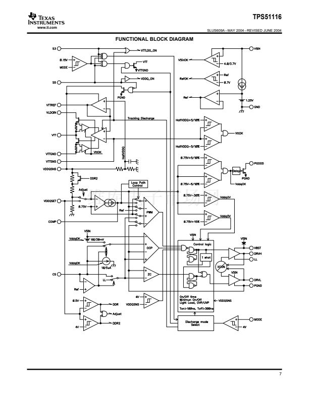
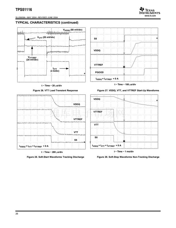
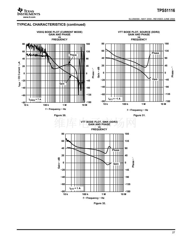
TPS51116
www.ti.com
SLUS609A 鈥?MAY 2004 鈥?REVISED JUNE 2004
APPLICATION INFORMATION (continued)
f
0
+
2p
1
ESR
C
O
v
f
SW
3
(24)
As f
0
is determined solely by the output capacitor鈥檚 characteristics, loop stability of D-CAP鈩?mode is determined
by the capacitor鈥檚 chemistry. For example, specialty polymer capacitors (SP-CAP) have C
O
in the order of
several 100 碌F and ESR in range of 10 m鈩? These makes f
0
in the order of 100 kHz or less and the loop is then
stable. However, ceramic capacitors have f
0
at more than 700 kHz, which is not suitable for this operational
mode.
Although D-CAP鈩?mode provides many advantages such as ease-of-use, minimum external components
configuration and extremely short response time, due to not employing an error amplifier in the loop, sufficient
amount of feedback signal needs to be provided by external circuit to reduce jitter level.
The required signal level is approximately 15 mV at comparing point. This gives V
RIPPLE
= (V
OUT
/0.75) x 15 (mV)
at the output node. The output capacitor鈥檚 ESR should meet this requirement.
The external components selection is much simple in D-CAP鈩?mode.
1.
Choose inductor.
This section is the same as the current mode. Please refer to the instructions in the
Current Mode Operation
section.
2.
Choose output capacitor(s).Organic
semiconductor capacitor(s) or specialty polymer capacitor(s) are
recommended. Determine ESR to meet required ripple voltage above. A quick approximation is shown in
Equation 25.
V
0.015
ESR
+
OUT
[
V
OUT
60 [mW]
I
RIPPLE
0.75
I
OUT(max)
(25)
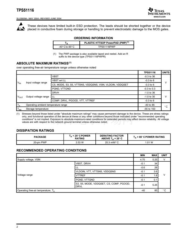
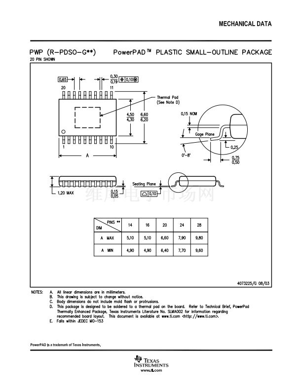
Thermal Design
Primary power dissipation of TPS51116 is generated from VTT regulator. VTT current flow in both source and
sink directions generate power dissipation from the part. In the source phase, potential difference between
VLDOIN and VTT times VTT current becomes the power dissipation, W
DSRC
.
W
DSRC
+
V
VLDOIN
*
V
VTT
I
VTT
(26)
In this case, if VLDOIN is connected to an alternative power supply lower than VDDQ voltage, power loss can be
decreased.
For the sink phase, VTT voltage is applied across the internal LDO regulator, and the power dissipation, W
DSNK
,
is calculated by Equation 27:
W
DSNK
+
V
VTT
I
VTT
(27)
Since this device does not sink AND source the current at the same time and I
VTT
varies rapidly with time, actual
power dissipation need to be considered for thermal design is an average of above value. Another power
consumption is the current used for internal control circuitry from V5IN supply and VLDOIN supply. V5IN
supports both the internal circuit and external MOSFETs drive current. The former current is in the VLDOIN
supply can be estimated as 1.5 mA or less at normal operational conditions.
These powers need to be effectively dissipated from the package. Maximum power dissipation allowed to the
package is calculated by Equation 28,
T
J(max)
*
T
A(max)
W
PKG
+
q
JA
(28)
where
鈥?/div>
T
J(max)
is 125掳C
鈥?/div>
T
A(max)
is the maximum ambient temperature in the system
鈥?胃
JA
is the thermal resistance from the silicon junction to the ambient
17


 1
1
 2
2
 3
3
 4
4
 5
5
 6
6
 7
7
 8
8
 9
9
 10
10
 11
11
 12
12
 13
13
 14
14
 15
15
 16
16
 17
17
 18
18
 19
19
 20
20
 21
21
 22
22
 23
23
 24
24
 25
25
 26
26
 27
27
 28
28
 29
29
