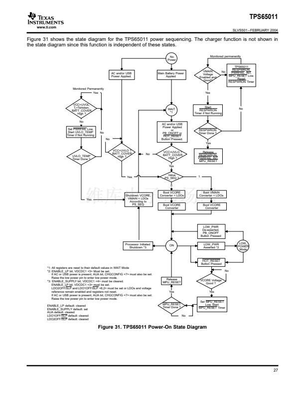
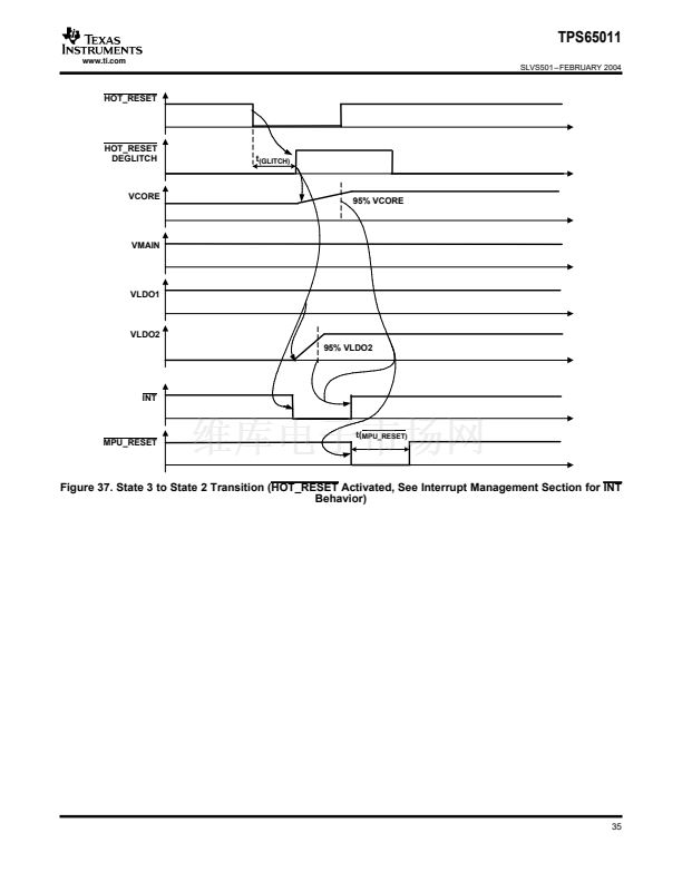
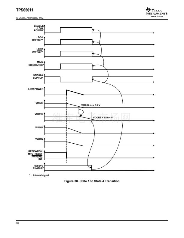
TPS65011
SLVS501 鈥?FEBRUARY 2004
www.ti.com
These devices have limited built-in ESD protection. The leads should be shorted together or the device placed in conductive foam
during storage or handling to prevent electrostatic damage to the MOS gates.
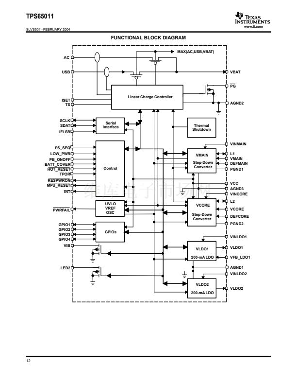
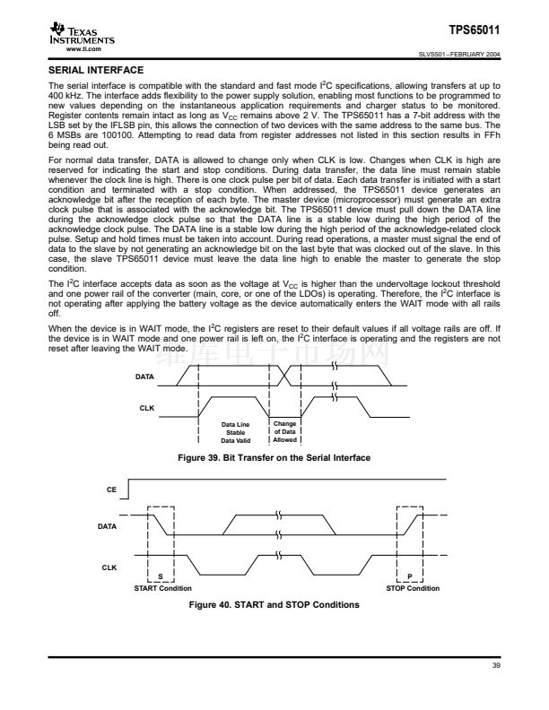
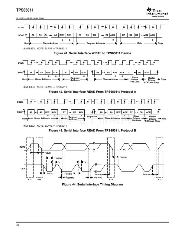
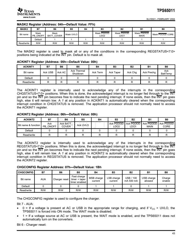
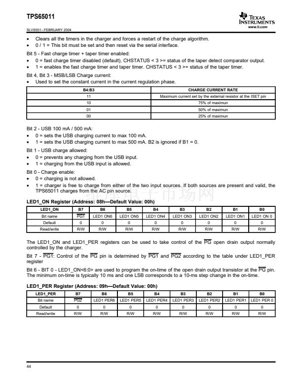
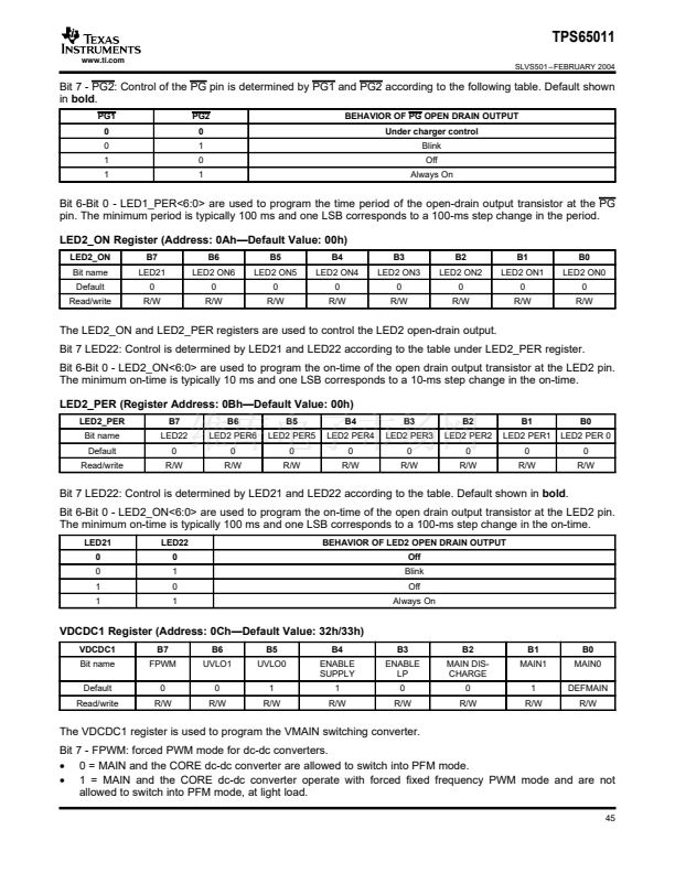
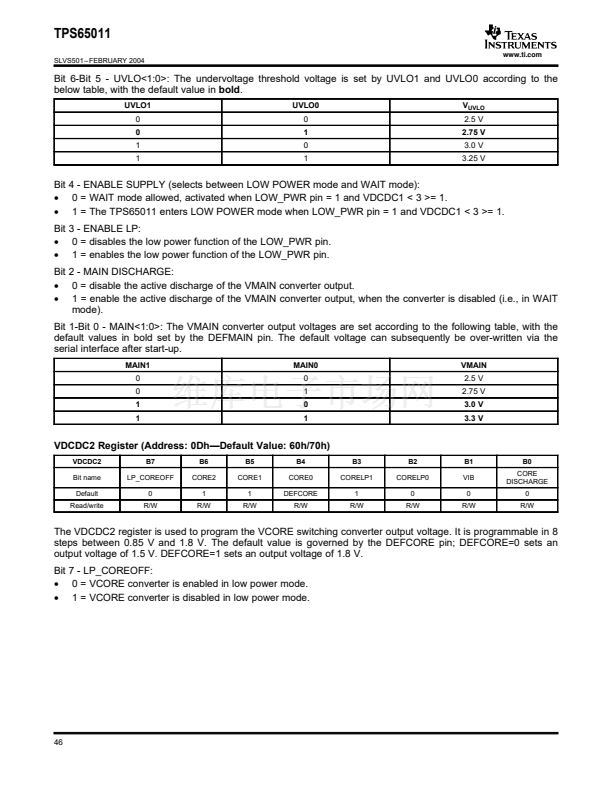
The serial interface can be used for dynamic voltage scaling, for collecting information on and controlling the
battery charger status, for optionally controlling 2 LED driver outputs, a vibrator driver, masking interrupts, or for
disabling/enabling and setting the LDO output voltages. The interface is compatible with the fast/standard mode
I
2
C鈩?specification allowing transfers at up to 400 kHz.
ORDERING INFORMATION
T
A
-40掳C to 85掳C
(1)
PACKAGE
7 mm
脳
7 mm, 48-pin QFN
PART NUMBER
(1)
TPS65011RGZ
The RGZ package is available in tape and reel. Add R suffix (TPS65011RGZR) to order quantities of
2500 parts per reel.
ABSOLUTE MAXIMUM RATINGS
over operating free-air temperature range unless otherwise noted
(1)
UNIT
Input voltage on VAC pin with respect to AGND
Input voltage range on all other pins except AGND/PGND pins with respect to AGND
HBM and CDM capabilities at pins VIB, PG, and LED2
Current at AC, VBAT, VINMAIN, L1, PGND1
Peak current at all other pins
Continuous power dissipation
Operating free-air temperature, T
A
Maximum junction temperature, T
J
Storage temperature, T
stg
Lead temperature 1,6 mm (1/16 inch) from case for 10 seconds
(1)
20 V
-0.3 V to 7 V
1 kV
1800 mA
1000 mA
See Dissipation Rating Table
-40掳C to 85掳C
125掳C
-65掳C to 150掳C
260掳C
Stresses beyond those listed under
absolute maximum ratings
may cause permanent damage to the device. These are stress ratings
only, and functional operation of the device at these or any other conditions beyond those indicated under
recommended operating
conditions
is not implied. Exposure to absolute-maximum-rated conditions for extended periods may affect device reliability.
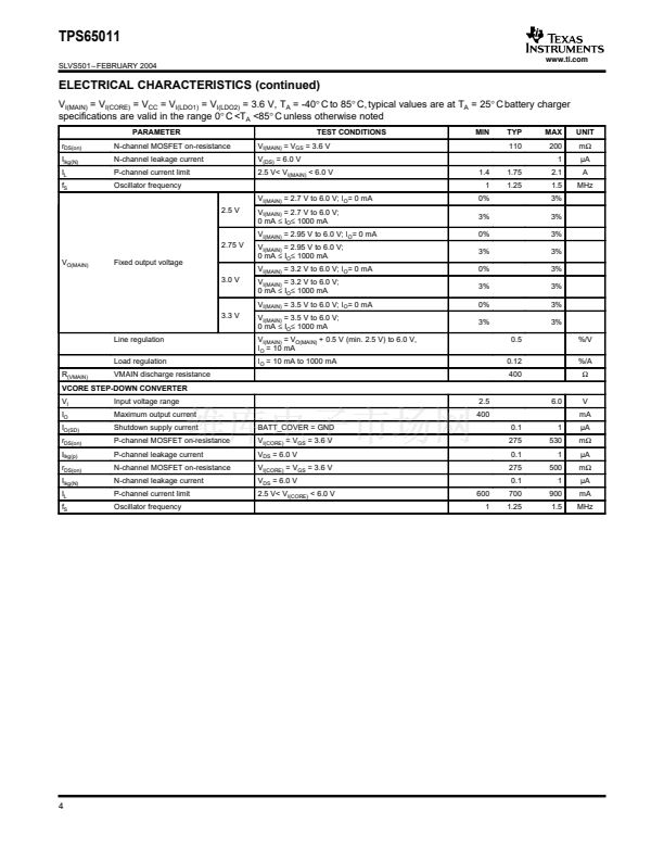
PACKAGE DISSIPATION RATINGS
(1)
AMBIENT
TEMPERATURE
25掳C
55掳C
(1)
(2)
MAX POWER DISSIPATION
FOR T
j
= 125掳C
(2)
3W
2.1 W
DERATING FACTOR
ABOVE T
A
= 55掳C
30 mW/掳C
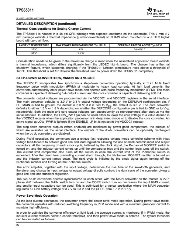
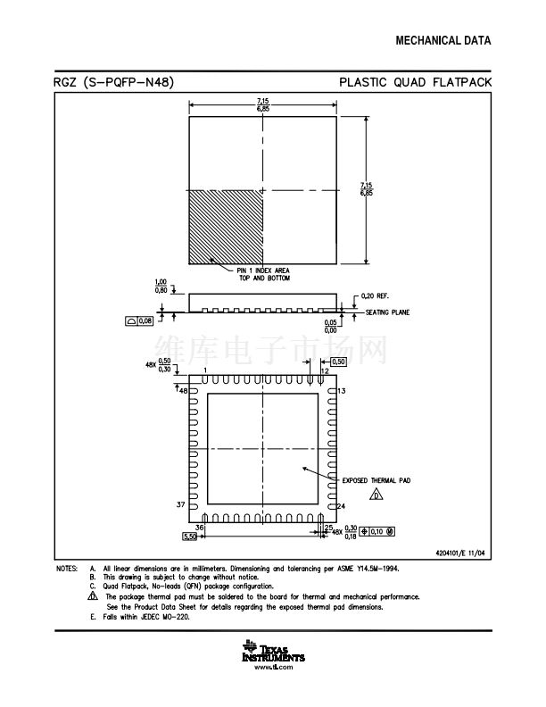
The TPS65011 is housed in a 48-pin QFN package with exposed leadframe on the underside. This
7 mm
脳
7 mm package exhibits a thermal impedance (junction-to-ambient) of 33 K/W when mounted
on a JEDEC high-k board.
Consideration needs to be given to the maximum charge current when the assembled application
board exhibits a thermal impedance which differs significantly from the JEDEC high-k board.
2


 1
1
 2
2
 3
3
 4
4
 5
5
 6
6
 7
7
 8
8
 9
9
 10
10
 11
11
 12
12
 13
13
 14
14
 15
15
 16
16
 17
17
 18
18
 19
19
 20
20
 21
21
 22
22
 23
23
 24
24
 25
25
 26
26
 27
27
 28
28
 29
29
 30
30
 31
31
 32
32
 33
33
 34
34
 35
35
 36
36
 37
37
 38
38
 39
39
 40
40
 41
41
 42
42
 43
43
 44
44
 45
45
 46
46
 47
47
 48
48
 49
49
 50
50
 51
51
 52
52
