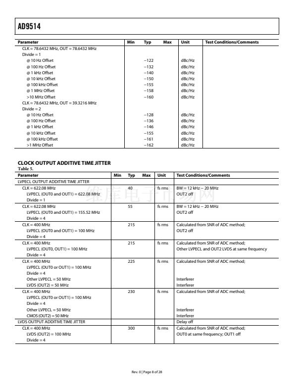
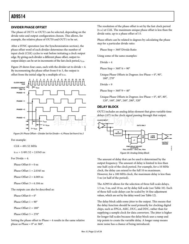
1.6 GHz Clock Distribution IC,
Dividers, Delay Adjust, Three Outputs
AD9514
FEATURES
1.6 GHz differential clock input
3 programmable dividers
Divide-by in range from1 to 32
Phase select for coarse delay adjust
2 independent 1.6 GHz LVPECL clock outputs
Additive broadband output jitter 225 fs rms
1 independent 800 MHz/250 MHz LVDS/CMOS clock output
Additive broadband output jitter 300 fs rms/290 fs rms
Time delays up to 10 ns
Device configured with 4-level logic pins
Space-saving, 32-lead LFCSP
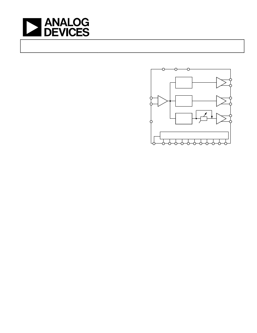
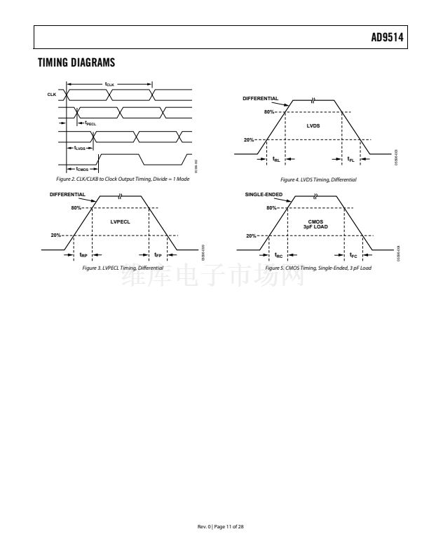
FUNCTIONAL BLOCK DIAGRAM
RSET
VS
GND
AD9514
/1. . . /32
LVPECL
OUT0
OUT0B
LVPECL
CLK
CLKB
/1. . . /32
OUT1
OUT1B
LVDS/CMOS
OUT2
SYNCB
/1. . . /32
螖
t
OUT2B
APPLICATIONS
Low jitter, low phase noise clock distribution
Clocking high speed ADCs, DACs, DDSs, DDCs, DUCs, MxFEs
High performance wireless transceivers
High performance instrumentation
Broadband infrastructure
ATE
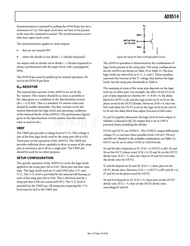
SETUP LOGIC
05596-001
VREF
S10
S9
S8
S7
S6
S5
S4
S3
S2
S1
S0
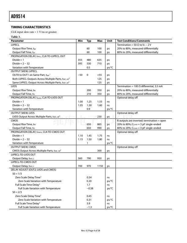
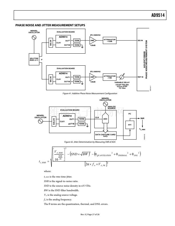
Figure 1.
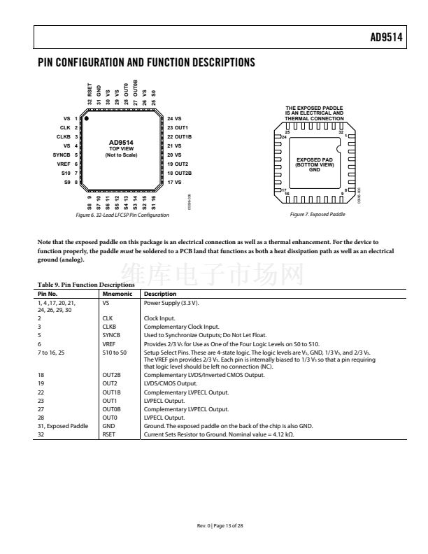
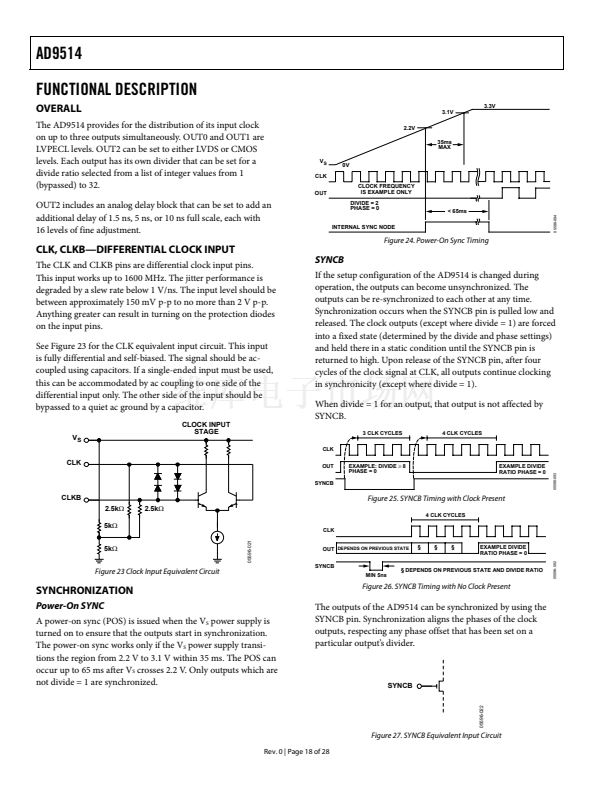
GENERAL DESCRIPTION
The AD9514 features a multi-output clock distribution IC in a
design that emphasizes low jitter and phase noise to maximize
data converter performance. Other applications with demanding
phase noise and jitter requirements also benefit from this part.
There are three independent clock outputs. Two of the outputs
are LVPECL, and the third output can be set to either LVDS or
CMOS levels. The LVPECL outputs operate to 1.6 GHz, and the
third output operates to 800 MHz in LVDS mode and to
250 MHz in CMOS mode.
Each output has a programmable divider that can be set to
divide by a selected set of integers ranging from 1 to 32. The
phase of one clock output relative to another clock output can
be set by means of a divider phase select function that serves as
a coarse timing adjustment.
The LVDS/CMOS output features a delay element with three
selectable full-scale delay values (1.5 ns, 5 ns, and 10 ns), each
with 16 steps of fine adjustment.
The AD9514 does not require an external controller for
operation or setup. The device is programmed by means of
11 pins (S0 to S10) using 4-level logic. The programming pins
are internally biased to 鈪?V
S
. The VREF pin provides a level of
鈪?V
S
. V
S
(3.3 V) and GND (0 V) provide the other two logic levels.
The AD9514 is ideally suited for data converter clocking
applications where maximum converter performance is
achieved by encode signals with subpicosecond jitter.
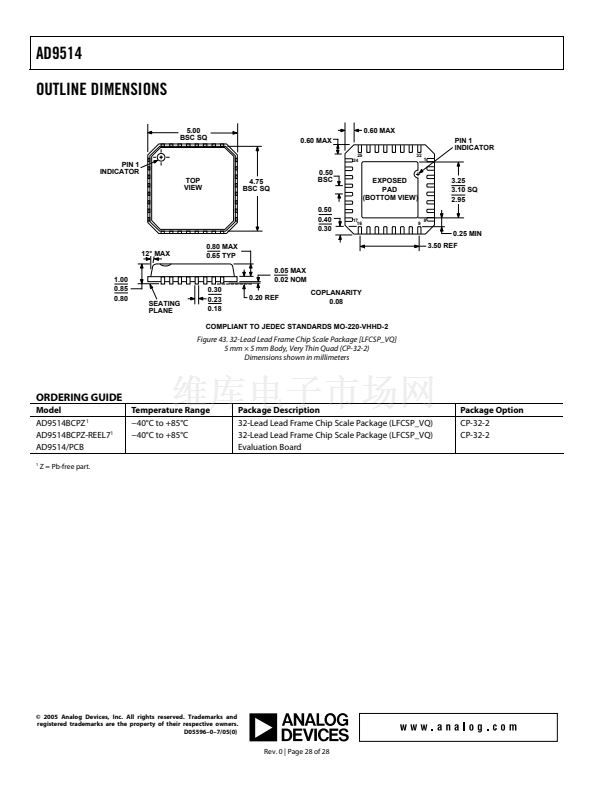
The AD9514 is available in a 32-lead LFCSP and operates from
a single 3.3 V supply. The temperature range is 鈭?0掳C to +85掳C.
Rev. 0
Information furnished by Analog Devices is believed to be accurate and reliable. However, no
responsibility is assumed by Analog Devices for its use, nor for any infringements of patents or other
rights of third parties that may result from its use. Specifications subject to change without notice. No
license is granted by implication or otherwise under any patent or patent rights of Analog Devices.
Trademarks and registered trademarks are the property of their respective owners.
One Technology Way, P.O. Box 9106, Norwood, MA 02062-9106, U.S.A.
Tel: 781.329.4700
www.analog.com
Fax: 781.461.3113
漏 2005 Analog Devices, Inc. All rights reserved.


 1
1
 2
2
 3
3
 4
4
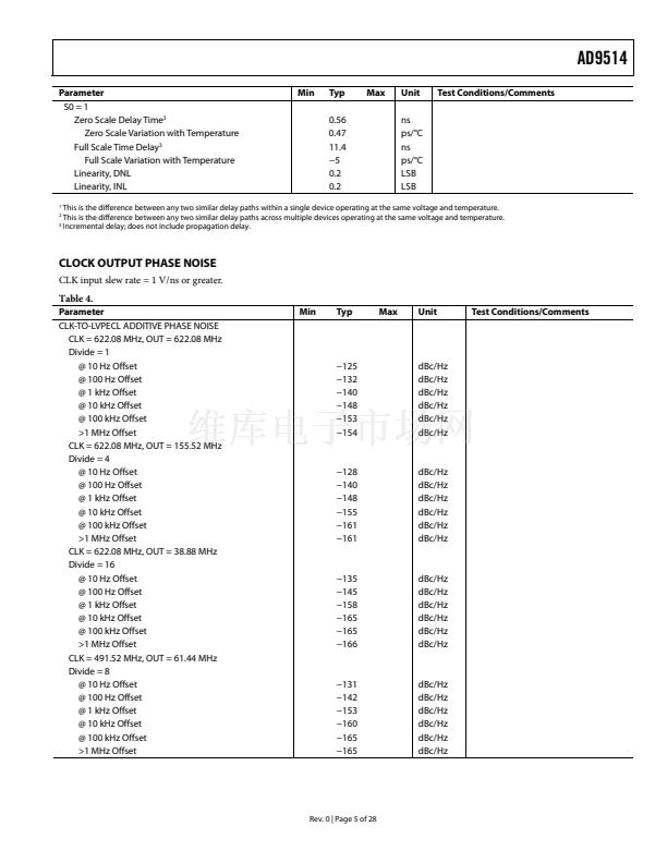 5
5
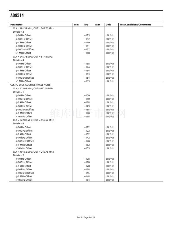 6
6
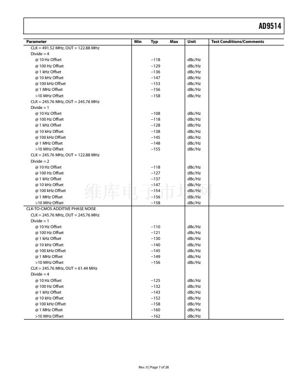 7
7
 8
8
 9
9
 10
10
 11
11
 12
12
 13
13
 14
14
 15
15
 16
16
 17
17
 18
18
 19
19
 20
20
 21
21
 22
22
 23
23
 24
24
 25
25
 26
26
 27
27
 28
28
