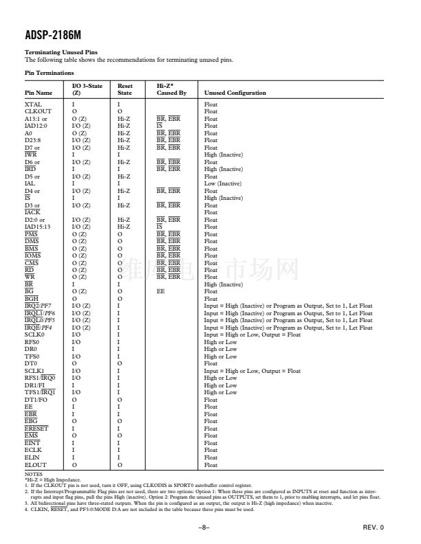
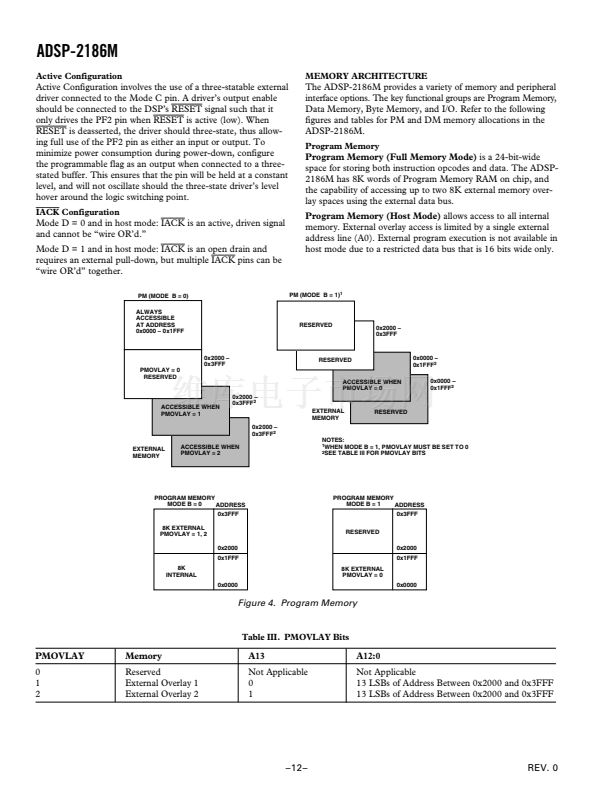
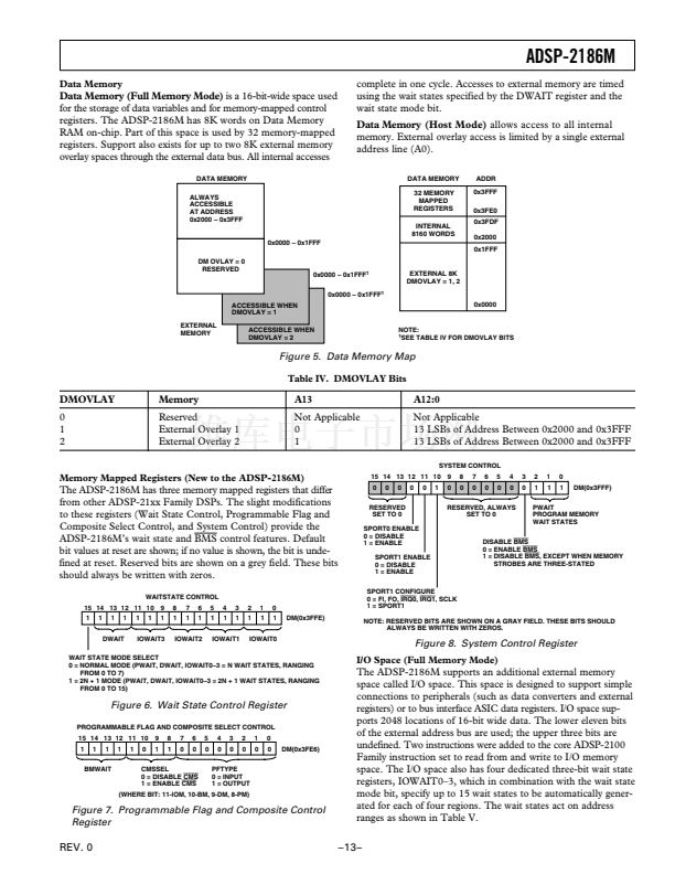
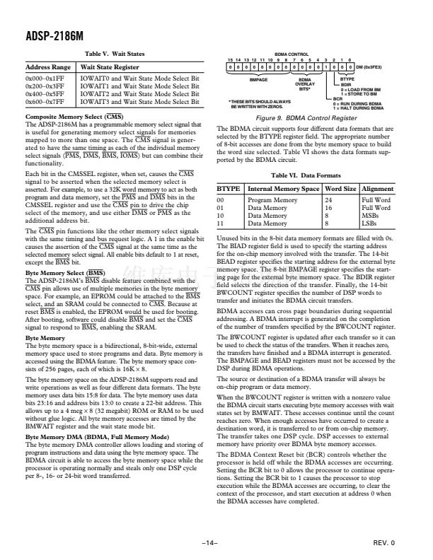
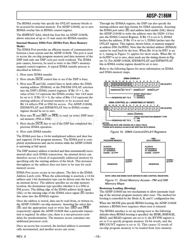
a
FEATURES
Performance
13.3 ns Instruction Cycle Time @ 2.5 V (Internal),
75 MIPS Sustained Performance
Single-Cycle Instruction Execution
Single-Cycle Context Switch
3-Bus Architecture Allows Dual Operand Fetches in
Every Instruction Cycle
Multifunction Instructions
Power-Down Mode Featuring Low CMOS Standby Power
Dissipation with 200 CLKIN Cycle Recovery from
Power-Down Condition
Low Power Dissipation in Idle Mode
DSP
Microcomputer
ADSP-2186M
System Interface
Flexible I/O Structure Allows 2.5 V or 3.3 V Operation;
All Inputs Tolerate up to 3.6 V Regardless of Mode
16-Bit Internal DMA Port for High-Speed Access to
On-Chip Memory (Mode Selectable)
4 MByte Memory Interface for Storage of Data Tables
and Program Overlays (Mode Selectable)
8-Bit DMA to Byte Memory for Transparent Program
and Data Memory Transfers (Mode Selectable)
I/O Memory Interface with 2048 Locations Supports
Parallel Peripherals (Mode Selectable)
Programmable Memory Strobe and Separate I/O
Memory Space Permits 鈥淕lueless鈥?System Design
Programmable Wait State Generation
Two Double-Buffered Serial Ports with Companding
Hardware and Automatic Data Buffering
Automatic Booting of On-Chip Program Memory from
Byte-Wide External Memory, e.g., EPROM, or
through Internal DMA Port
Six External Interrupts
13 Programmable Flag Pins Provide Flexible System
Signaling
UART Emulation through Software SPORT Reconfiguration
ICE-Port鈩?Emulator Interface Supports Debugging in
Final Systems
Integration
ADSP-2100 Family Code Compatible (Easy to Use
Algebraic Syntax), with Instruction Set Extensions
40K Bytes of On-Chip RAM, Configured as
8K Words Program Memory RAM
8K Words Data Memory RAM
Dual-Purpose Program Memory for Both Instruction and
Data Storage
Independent ALU, Multiplier/Accumulator, and Barrel
Shifter Computational Units
Two Independent Data Address Generators
Powerful Program Sequencer Provides Zero Overhead
Looping Conditional Instruction Execution
Programmable 16-Bit Interval Timer with Prescaler
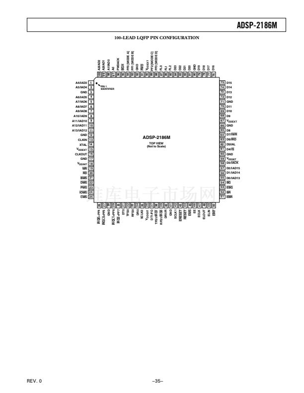
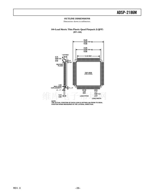
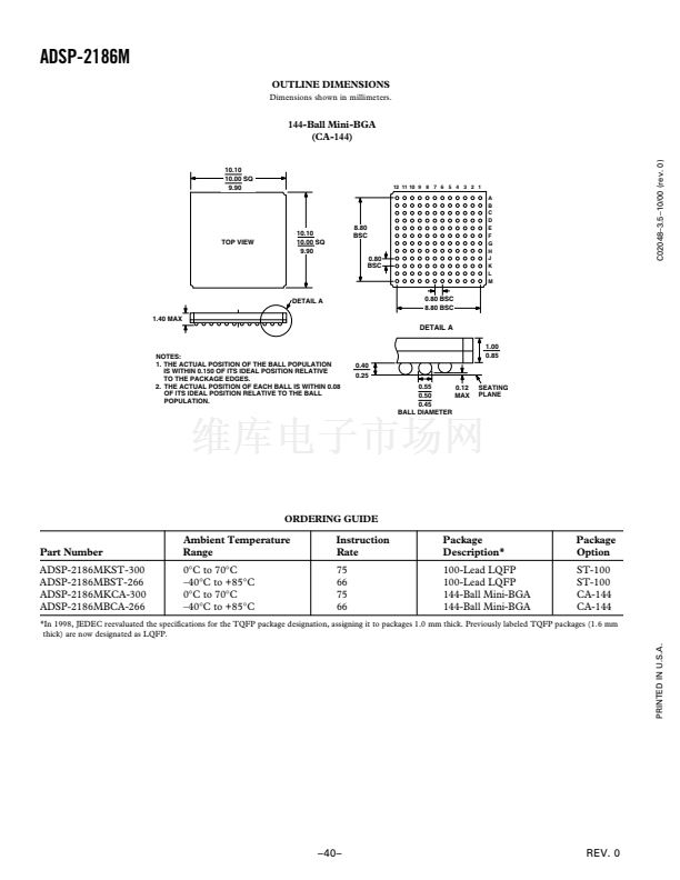
100-Lead LQFP and 144-Ball Mini-BGA
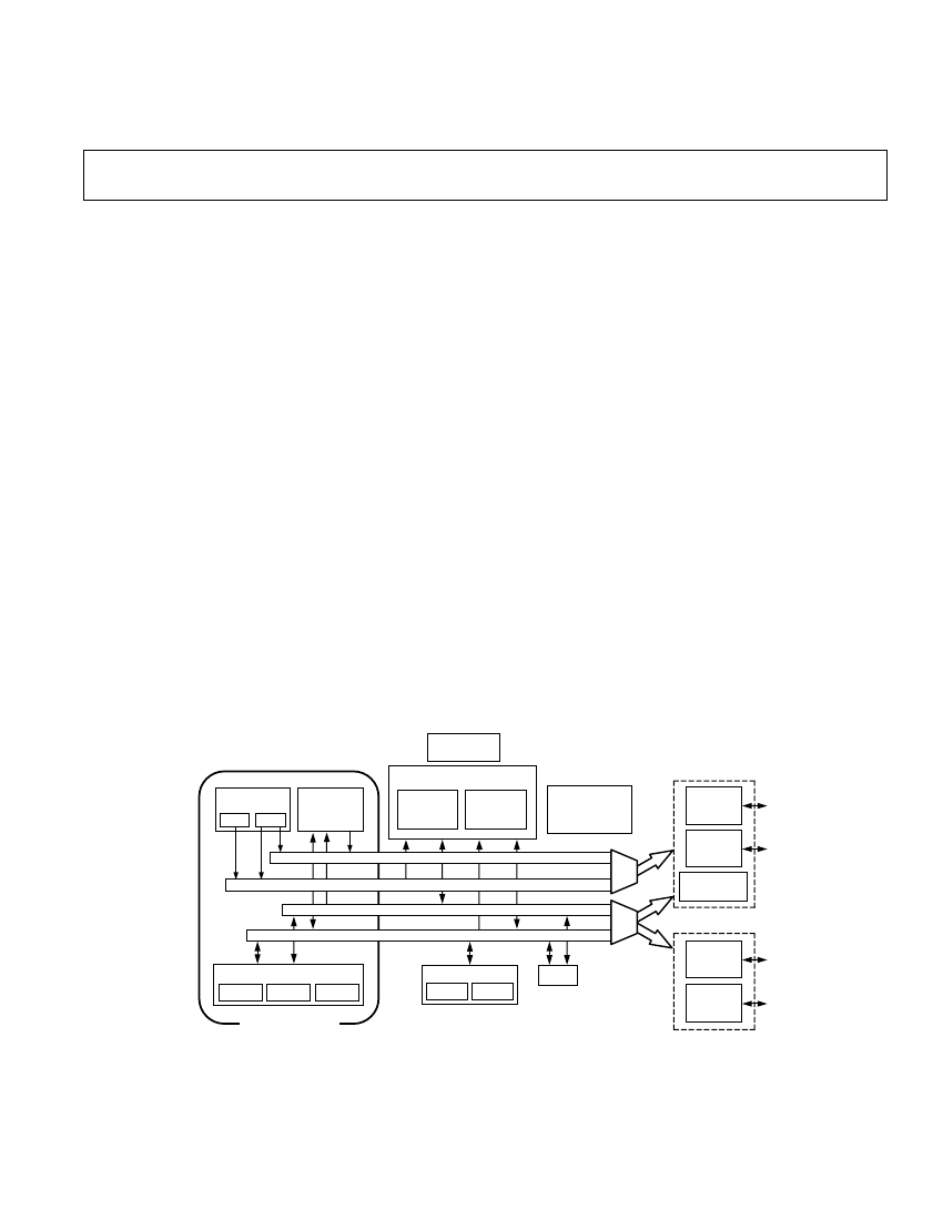
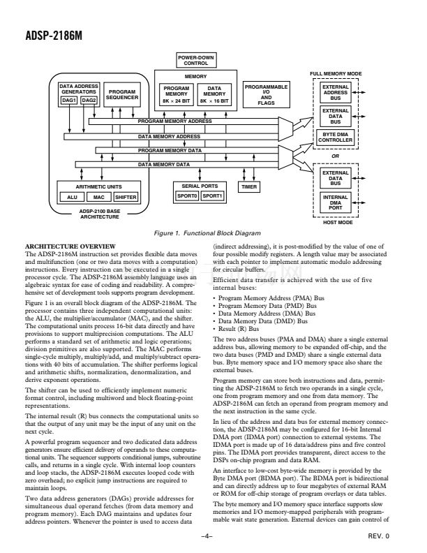
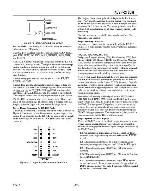
FUNCTIONAL BLOCK DIAGRAM
POWER-DOWN
CONTROL
MEMORY
FULL MEMORY MODE
PROGRAMMABLE
I/O
AND
FLAGS
DATA ADDRESS
GENERATORS
DAG1
DAG2
PROGRAM
SEQUENCER
PROGRAM
MEMORY
8K 24 BIT
DATA
MEMORY
8K
16 BIT
EXTERNAL
ADDRESS
BUS
EXTERNAL
DATA
BUS
BYTE DMA
CONTROLLER
PROGRAM MEMORY ADDRESS
DATA MEMORY ADDRESS
PROGRAM MEMORY DATA
OR
DATA MEMORY DATA
ARITHMETIC UNITS
ALU
MAC
SHIFTER
SERIAL PORTS
TIMER
EXTERNAL
DATA
BUS
INTERNAL
DMA
PORT
HOST MODE
SPORT0
SPORT1
ADSP-2100 BASE
ARCHITECTURE
ICE-Port is a trademark of Analog Devices, Inc.
REV. 0
Information furnished by Analog Devices is believed to be accurate and
reliable. However, no responsibility is assumed by Analog Devices for its
use, nor for any infringements of patents or other rights of third parties
which may result from its use. No license is granted by implication or
otherwise under any patent or patent rights of Analog Devices.
One Technology Way, P.O. Box 9106, Norwood, MA 02062-9106, U.S.A.
Tel: 781/329-4700
World Wide Web Site: http://www.analog.com
Fax: 781/326-8703
漏 Analog Devices, Inc., 2000


 1
1
 2
2
 3
3
 4
4
 5
5
 6
6
 7
7
 8
8
 9
9
 10
10
 11
11
 12
12
 13
13
 14
14
 15
15
 16
16
 17
17
 18
18
 19
19
 20
20
 21
21
 22
22
 23
23
 24
24
 25
25
 26
26
 27
27
 28
28
 29
29
 30
30
 31
31
 32
32
 33
33
 34
34
 35
35
 36
36
 37
37
 38
38
 39
39
 40
40
