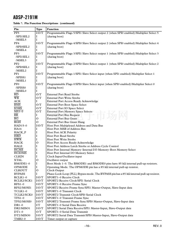
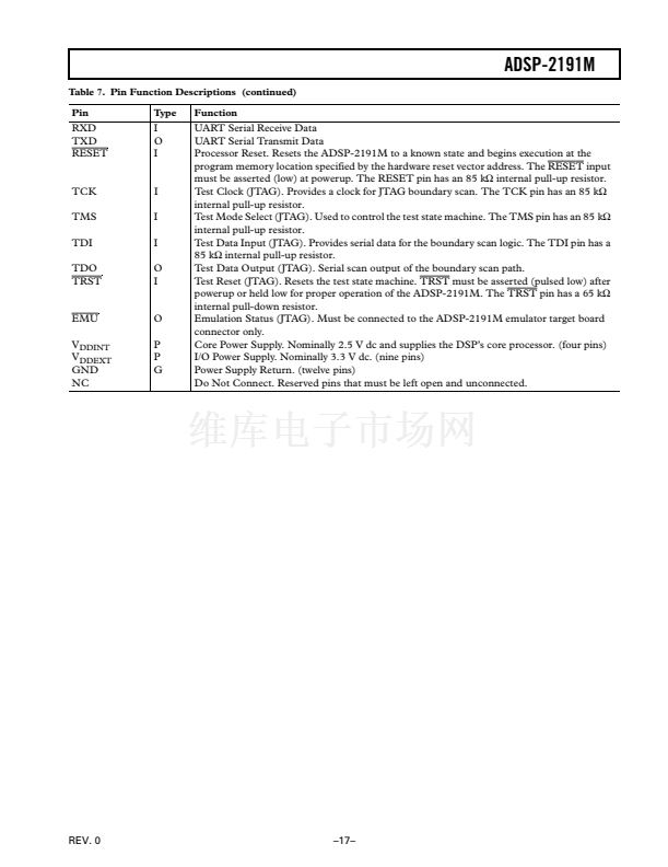
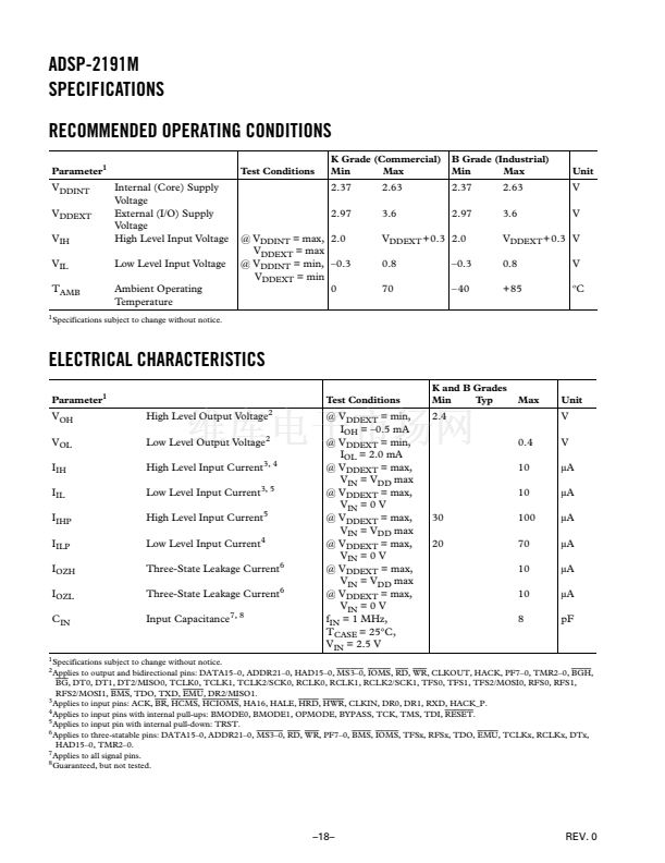
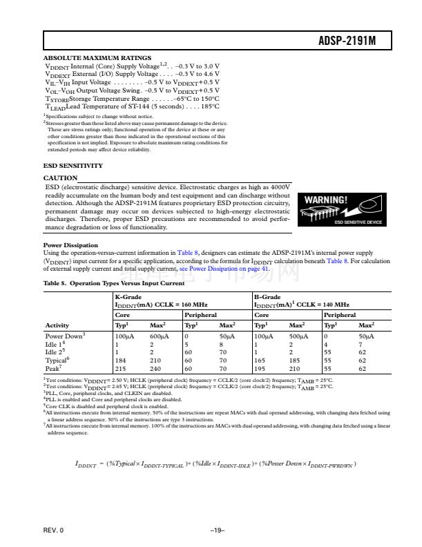
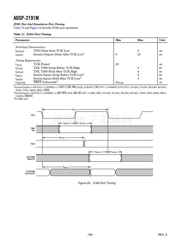
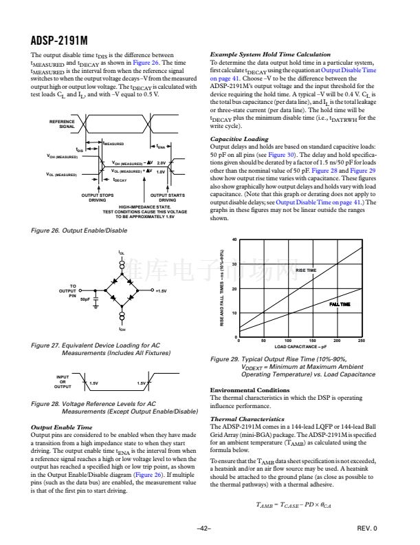
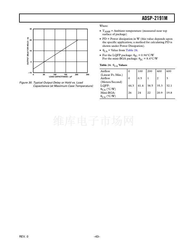
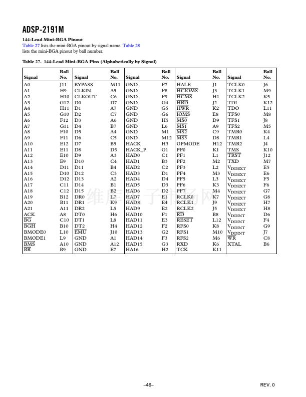
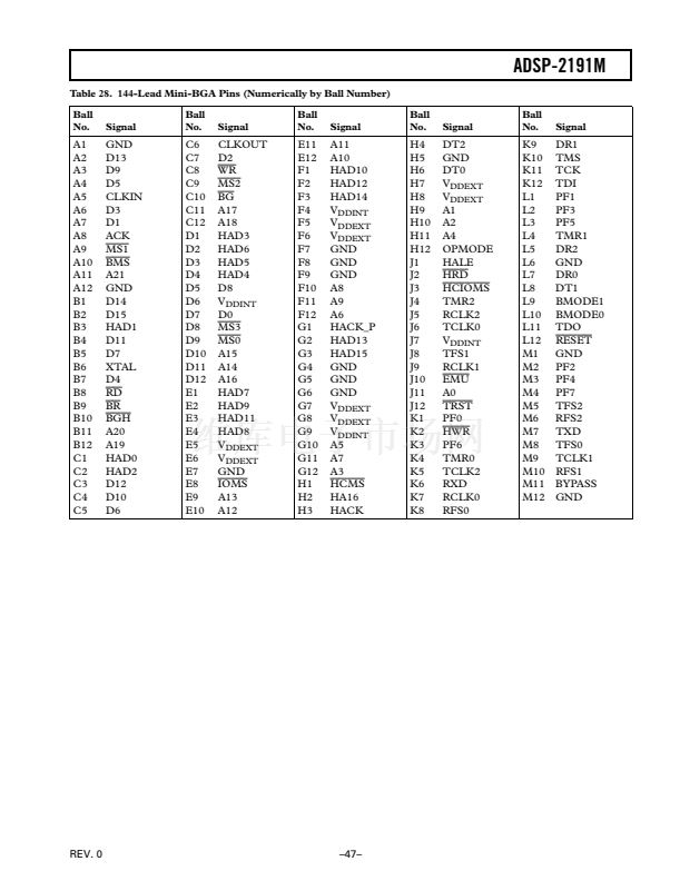
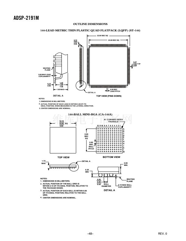
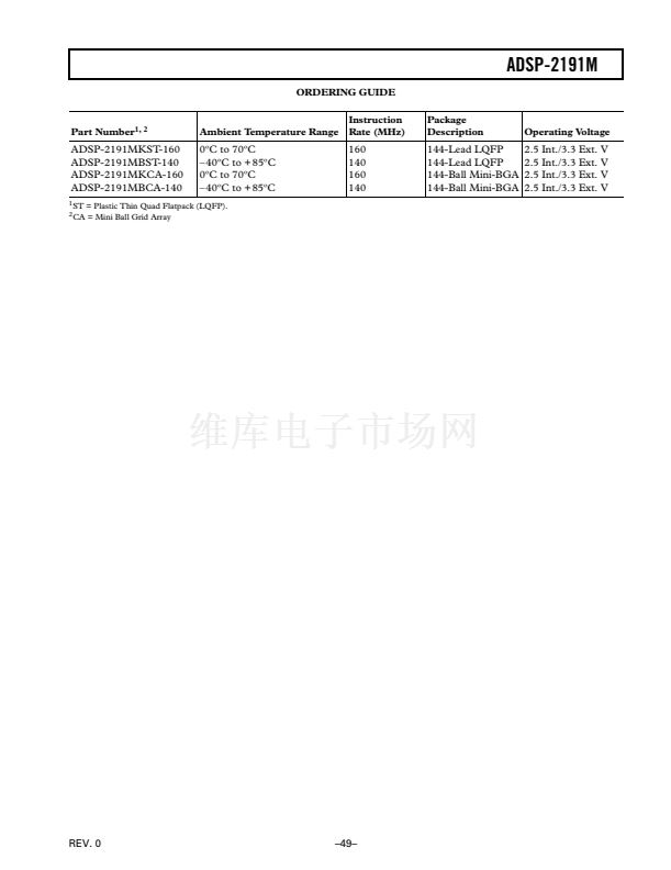
a
PERFORMANCE FEATURES
6.25 ns Instruction Cycle Time, for up to 160 MIPS
Sustained Performance
ADSP-218x Family Code Compatible with the Same
Easy to Use Algebraic Syntax
Single-Cycle Instruction Execution
Single-Cycle Context Switch between Two Sets of Com-
putation and Memory Instructions
Instruction Cache Allows Dual Operand Fetches in Every
Instruction Cycle
DSP Microcomputer
ADSP-2191M
Multifunction Instructions
Pipelined Architecture Supports Efficient Code
Execution
Architectural Enhancements for Compiled C and C++
Code Efficiency
Architectural Enhancements beyond ADSP-218x Family
are Supported with Instruction Set Extensions for
Added Registers, and Peripherals
Flexible Power Management with User-Selectable
Power-Down and Idle Modes
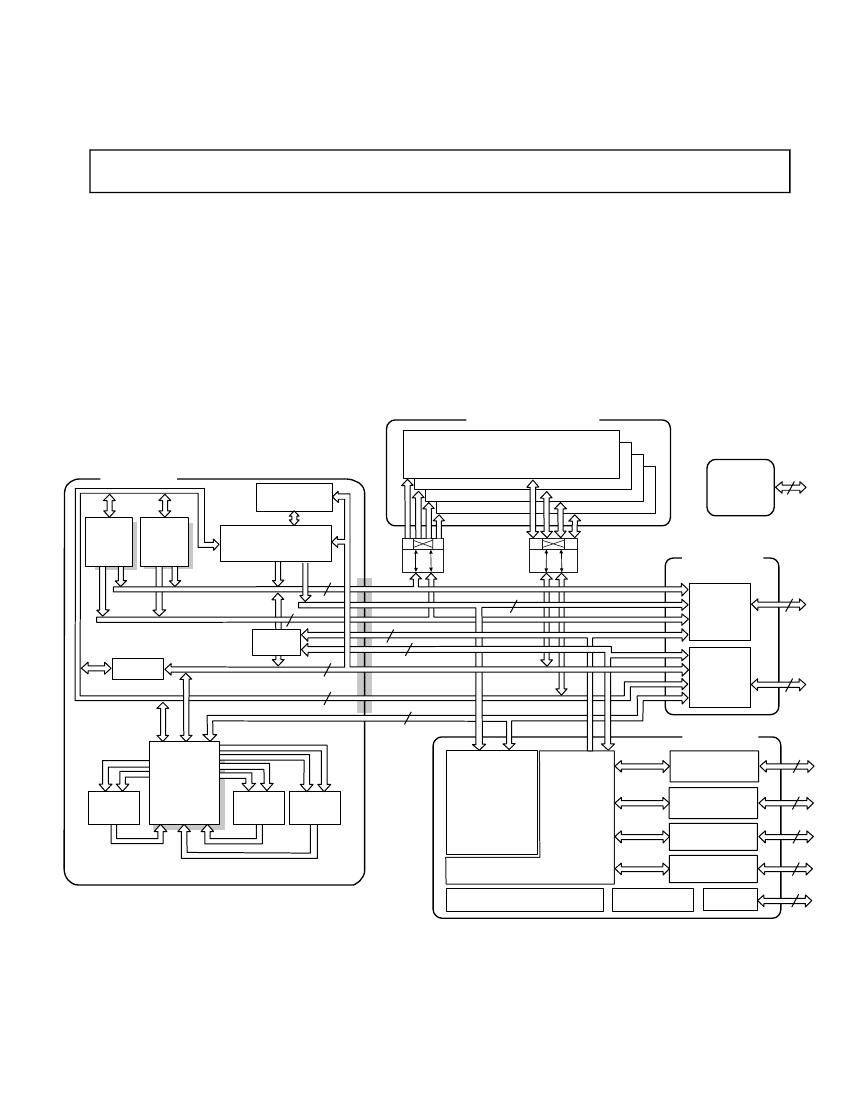
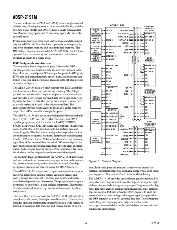
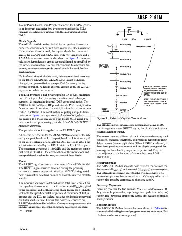
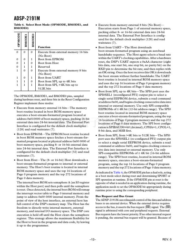
FUNCTIONAL BLOCK DIAGRAM
INTERNAL MEMORY
FOUR INDEPENDENT BLOCKS
ADSP-219x
DSP CORE
CACHE
64 24-BIT
BLOCK0
BLOCK1
BLOCK2
BLOCK3
24 BIT
ADDRESS
DATA
24 BIT
ADDRESS
DATA
16 BIT
DATA
ADDRESS
16 BIT
DATA
ADDRESS
JTAG
TEST &
EMULATION
6
4
DAG1
4 16
4
DAG2
4 16
PROGRAM
SEQUENCER
EXTERNAL PORT
PM ADDRESS BUS
24
I/O ADDRESS
18
ADDR BUS
MUX
24
DMA
CONNECT
PM DATA BUS
24
16
16
I/O DATA
I/O PROCESSOR
DATA BUS
MUX
16
DMA ADDRESS
24
DMA DATA
22
DM ADDRESS BUS
24
PX
DM DATA BUS
DATA
REGISTER
FILE
INPUT
REGISTERS
RESULT
REGISTERS
MULT
16
16-BIT
BARREL
SHIFTER
ALU
I/O REGISTERS
(MEMORY-MAPPED)
CONTROL
STATUS
BUFFERS
DMA
CONTROLLER
24
HOST PORT
18
SERIAL PORTS
(3)
6
SPI PORTS
(2)
2
UART PORT
(1)
3
SYSTEM INTERRUPT CONTROLLER
PROGRAMMABLE
FLAGS (16)
TIMERS (3)
REV. 0
Information furnished by Analog Devices is believed to be accurate and
reliable. However, no responsibility is assumed by Analog Devices for its
use, nor for any infringements of patents or other rights of third parties that
may result from its use. No license is granted by implication or otherwise
under any patent or patent rights of Analog Devices.
One Technology Way, P.O.Box 9106, Norwood, MA 02062-9106, U.S.A.
Tel:781/329-4700
www.analog.com
Fax:781/326-8703
漏
Analog Devices, Inc., 2002


 1
1
 2
2
 3
3
 4
4
 5
5
 6
6
 7
7
 8
8
 9
9
 10
10
 11
11
 12
12
 13
13
 14
14
 15
15
 16
16
 17
17
 18
18
 19
19
 20
20
 21
21
 22
22
 23
23
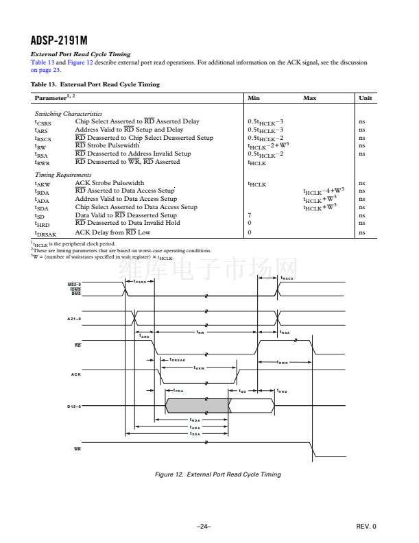 24
24
 25
25
 26
26
 27
27
 28
28
 29
29
 30
30
 31
31
 32
32
 33
33
 34
34
 35
35
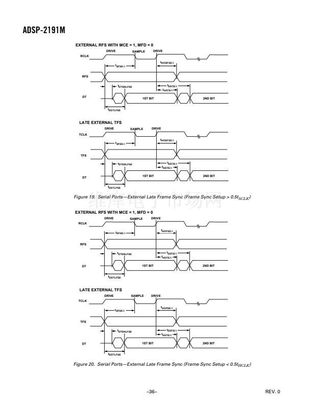 36
36
 37
37
 38
38
 39
39
 40
40
 41
41
 42
42
 43
43
 44
44
 45
45
 46
46
 47
47
 48
48
 49
49
 50
50
 51
51
 52
52
