鈥?/div>
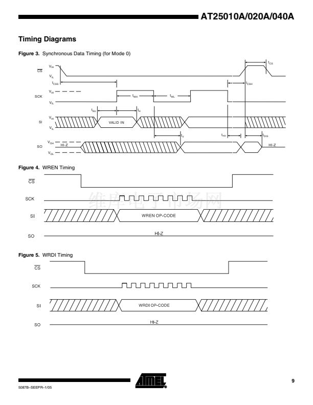
鈥?Data Sheet Describes Mode 0 Operation
Medium-voltage and Standard-voltage Operation
鈥?2.7 (V
CC
= 2.7V to 5.5V)
Extended Temperature Range
鈭?0掳C
to +125掳C
5.0 MHz Clock Rate
8-byte Page Mode
Block Write Protection
鈥?Protect 1/4, 1/2, or Entire Array
Write Protect (WP) Pin and Write Disable Instructions for Both Hardware and Software
Data Protection
Self-timed Write Cycle (10 ms max)
High Reliability
鈥?Endurance: One Million Write Cycles
鈥?Data Retention: 100 Years
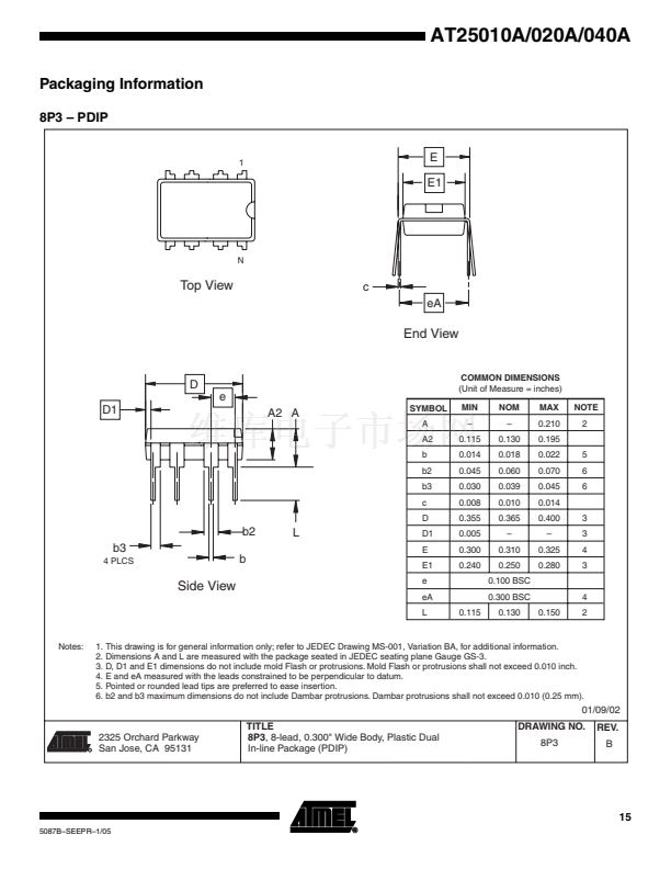
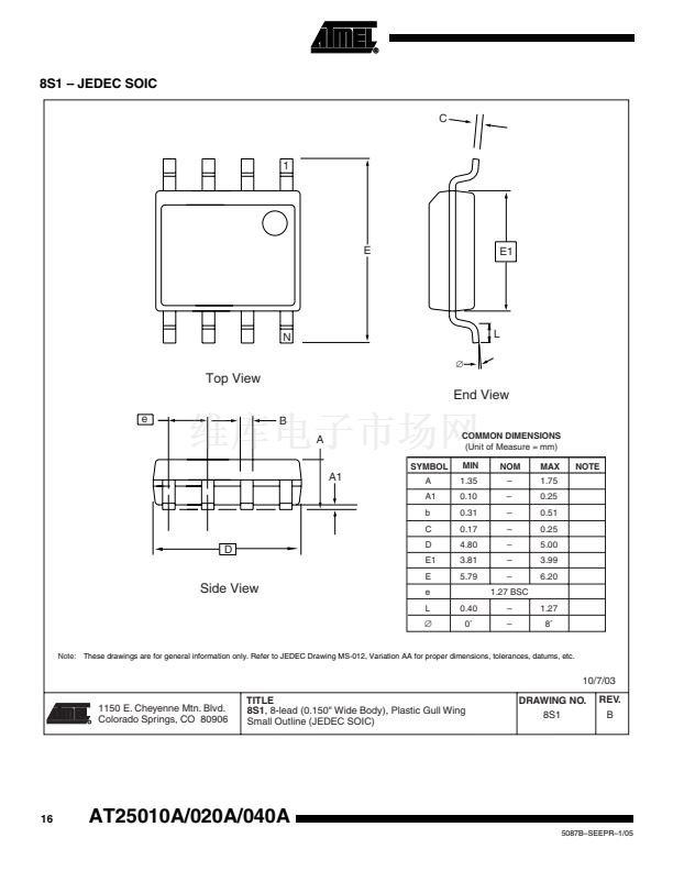
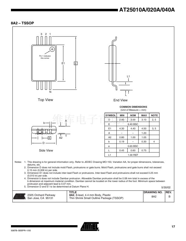
8-lead PDIP, 8-lead JEDEC SOIC, 8-lead TSSOP Packages
SPI Serial
Extended
Temperature
EEPROMs
1K (128 x 8)
2K (256 x 8)
4K (512 x 8)
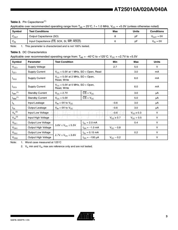
Description
The AT25010A/020A/040A provides 1024/2048/4096 bits of serial electrically-eras-
able programmable read-only memory (EEPROM) organized as 128/256/512 words of
8 bits each. The device is optimized for use in many automotive applications where
low-power and low-voltage operation are essential. The AT25010A/020A/040A is
available in space-saving 8-pin PDIP, 8-lead JEDEC SOIC and 8-lead TSSOP
packages.
The AT25010A/020A/040A is enabled through the Chip Select pin (CS) and accessed
via a three-wire interface consisting of Serial Data Input (SI), Serial Data Output (SO),
and Serial Clock (SCK). All programming cycles are completely self-timed, and no
separate erase cycle is required before write.
Block write protection is enabled by programming the status register with one of four
blocks of write protection. Separate program enable and program disable instructions
are provided for additional data protection. Hardware data protection is provided via
the WP pin to protect against inadvertent write attempts. The HOLD pin may be used
to suspend any serial communication without resetting the serial sequence.
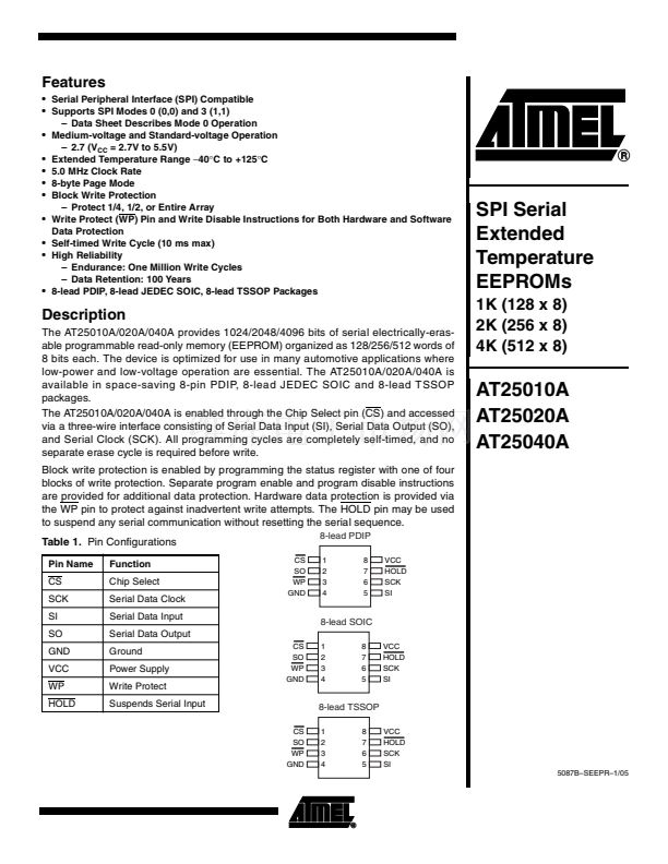
Table 1.
Pin Configurations
Pin Name
CS
SCK
SI
SO
GND
VCC
WP
HOLD
Function
Chip Select
Serial Data Clock
Serial Data Input
Serial Data Output
Ground
Power Supply
Write Protect
Suspends Serial Input
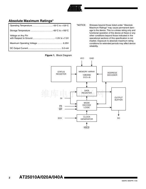
CS
SO
WP
GND
CS
SO
WP
GND
1
2
3
4
8
7
6
5
VCC
HOLD
SCK
SI
CS
SO
WP
GND
AT25010A
AT25020A
AT25040A
8-lead
PDIP
1
2
3
4
8
7
6
5
VCC
HOLD
SCK
SI
8-lead SOIC
8-lead
TSSOP
1
2
3
4
8
7
6
5
VCC
HOLD
SCK
SI
5087B鈥揝EEPR鈥?/05
1


 1
1
 2
2
 3
3
 4
4
 5
5
 6
6
 7
7
 8
8
 9
9
 10
10
 11
11
 12
12
 13
13
 14
14
 15
15
 16
16
 17
17
 18
18
