Sep. 2002
鈩?/div>
@V
GS
=10V.
Super high dense cell design for extremely low R
DS(ON)
.
High power and current handling capability.
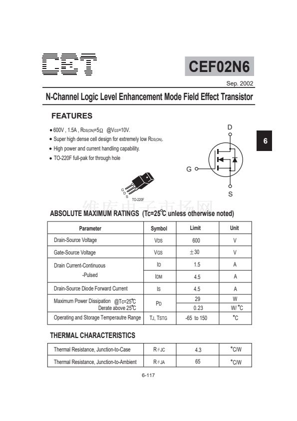
TO-220F full-pak for through hole
D
6
G
G
D
S
S
TO-220F
ABSOLUTE MAXIMUM RATINGS (Tc=25 C unless otherwise noted)
Parameter
Drain-Source Voltage
Gate-Source Voltage
Drain Current-Continuous
-Pulsed
Drain-Source Diode Forward Current
Maximum Power Dissipation
@Tc=25 C
Derate above 25 C
Operating and Storage Temperautre Range
Symbol
V
DS
V
GS
I
D
I
DM
I
S
P
D
T
J
, T
STG
Limit
600
30
1.5
4.5
4.5
29
0.23
-65 to 150
Unit
V
V
A
A
A
W
W/ C
C
THERMAL CHARACTERISTICS
Thermal Resistance, Junction-to-Case
Thermal Resistance, Junction-to-Ambient
R
JC
R
JA
6-117
4.3
65
C/W
C/W


 1
1
 2
2
 3
3
 4
4
 5
5
