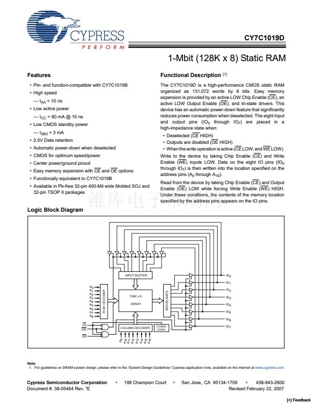
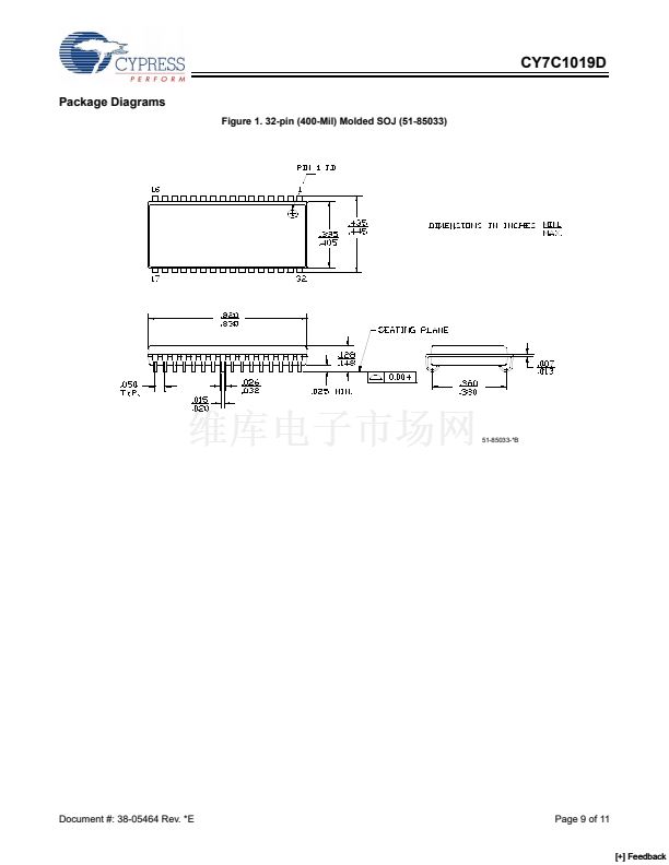
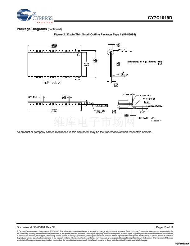
CY7C1019D
1-Mbit (128K x 8) Static RAM
Features
鈥?Pin- and function-compatible with CY7C1019B
鈥?High speed
鈥?t
AA
= 10 ns
鈥?Low active power
鈥?I
CC
= 80 mA @ 10 ns
鈥?Low CMOS standby power
鈥?I
SB2
= 3 mA
鈥?2.0V Data retention
鈥?Automatic power-down when deselected
鈥?CMOS for optimum speed/power
鈥?Center power/ground pinout
鈥?Easy memory expansion with CE and OE options
鈥?Functionally equivalent to CY7C1019B
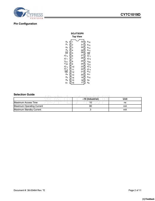
鈥?Available in Pb-free 32-pin 400-Mil wide Molded SOJ and
32-pin TSOP II packages
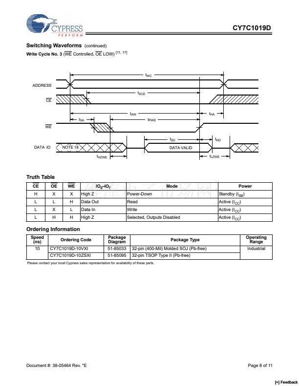
Functional Description
[1]
The CY7C1019D is a high-performance CMOS static RAM
organized as 131,072 words by 8 bits. Easy memory
expansion is provided by an active LOW Chip Enable (CE), an
active LOW Output Enable (OE), and tri-state drivers. This
device has an automatic power-down feature that significantly
reduces power consumption when deselected. The eight input
and output pins (IO
0
through IO
7
) are placed in a
high-impedance state when:
鈥?Deselected (CE HIGH)
鈥?Outputs are disabled (OE HIGH)
鈥?When the write operation is active (CE LOW, and WE LOW).
Write to the device by taking Chip Enable (CE) and Write
Enable (WE) inputs LOW. Data on the eight IO pins (IO
0
through IO
7
) is then written into the location specified on the
address pins (A
0
through A
16
).
Read from the device by taking Chip Enable (CE) and Output
Enable (OE) LOW while forcing Write Enable (WE) HIGH.
Under these conditions, the contents of the memory location
specified by the address pins appears on the IO pins.
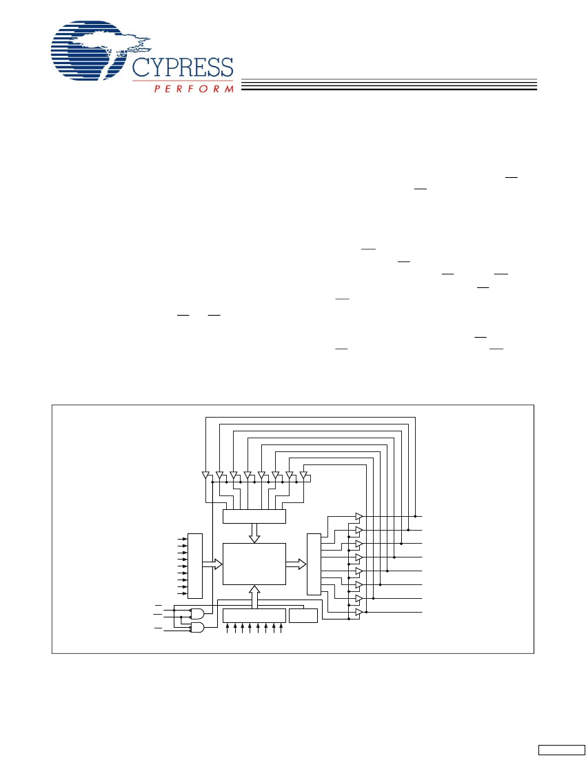
Logic Block Diagram
INPUT BUFFER
A0
A1
A2
A3
A4
A5
A6
A7
A8
CE
WE
OE
IO0
IO1
ROW DECODER
128K x 8
ARRAY
SENSE AMPS
IO2
IO3
IO4
IO5
IO6
COLUMN DECODER
POWER
DOWN
IO7
Note
1. For guidelines on SRAM system design, please refer to the 鈥楽ystem Design Guidelines鈥?Cypress application note, available on the internet at
www.cypress.com.
A9
A10
A11
A12
A13
A14
A15
A16
Cypress Semiconductor Corporation
Document #: 38-05464 Rev. *E
鈥?/div>
198 Champion Court
鈥?/div>
San Jose
,
CA 95134-1709
鈥?/div>
408-943-2600
Revised February 22, 2007
[+] Feedback


 1
1
 2
2
 3
3
 4
4
 5
5
 6
6
 7
7
 8
8
 9
9
 10
10
 11
11
