铮?/div>
interleaved or linear burst sequences
Separate processor and controller address strobes
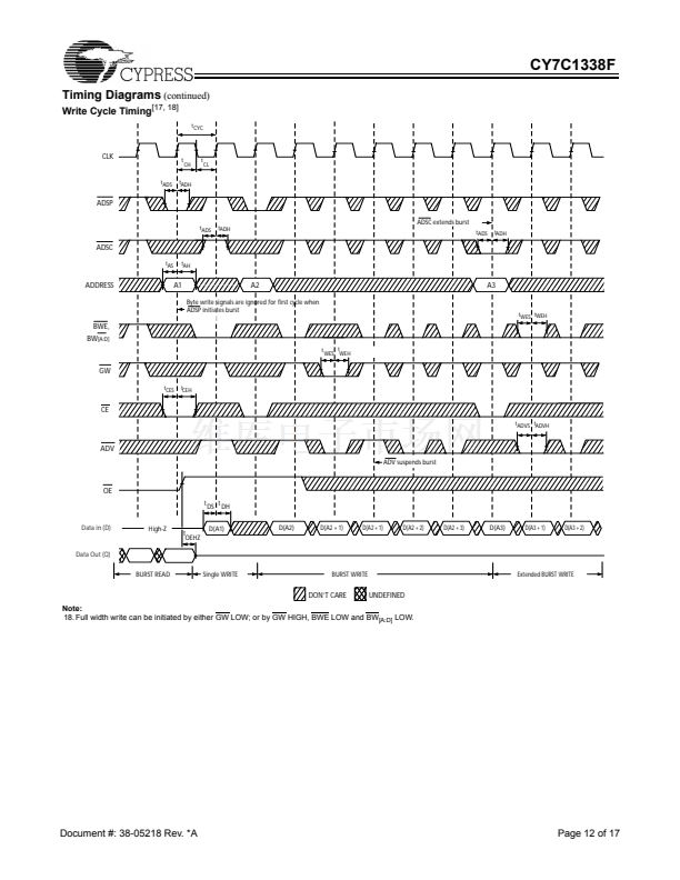
Synchronous self-timed write
Asynchronous output enable
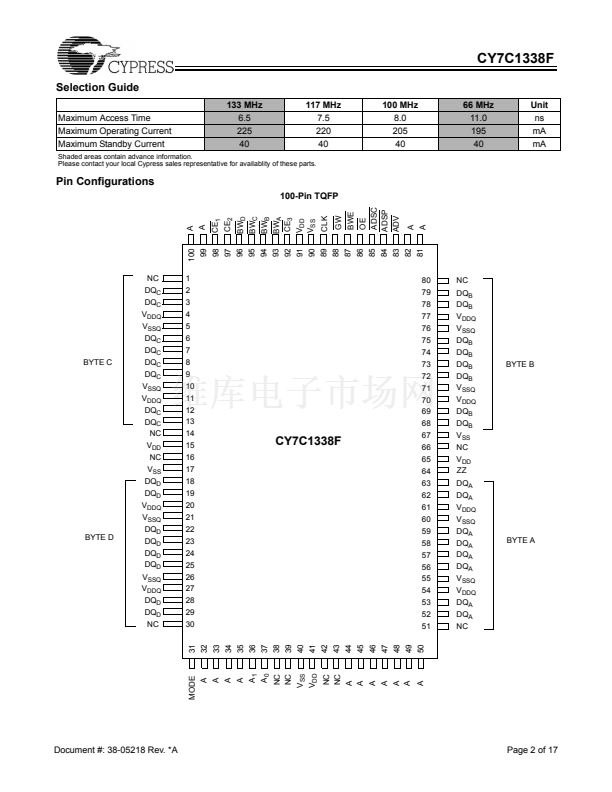
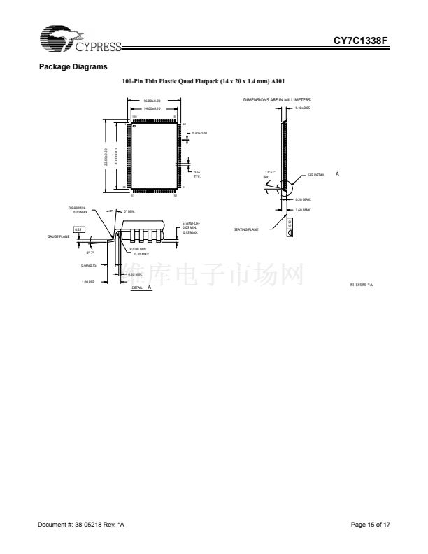
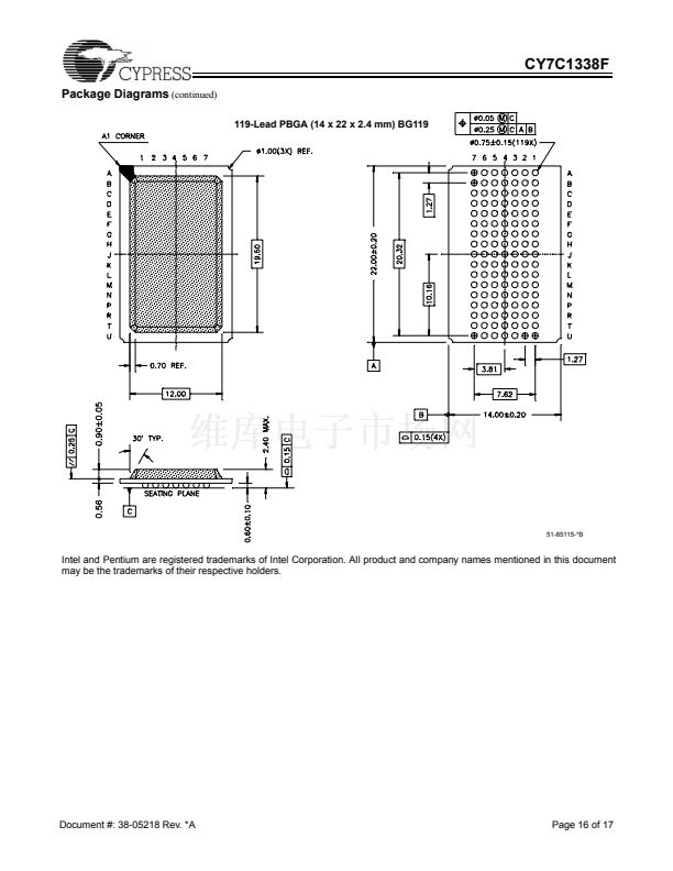
Offered in JEDEC-standard 100-pin TQFP and 119-ball
BGA packages
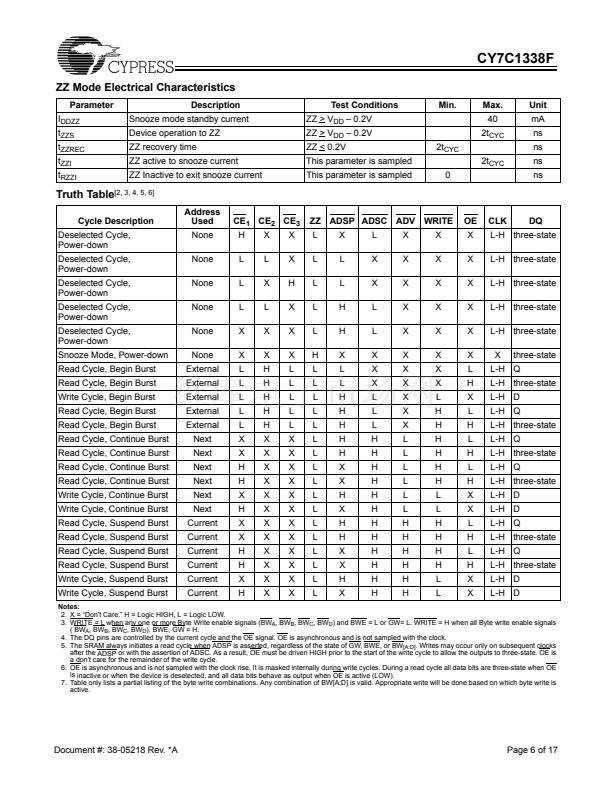
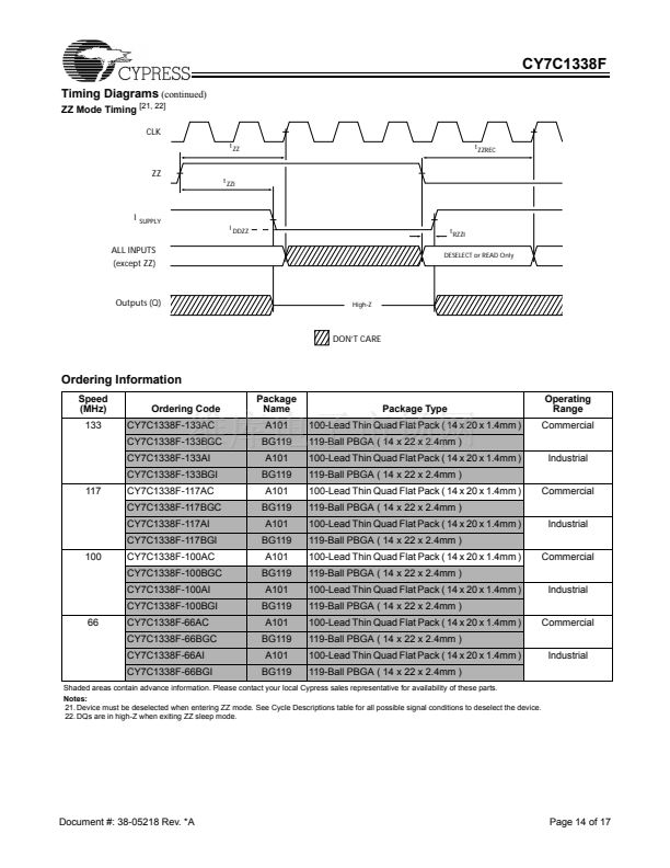
鈥淶Z鈥?Sleep Mode option
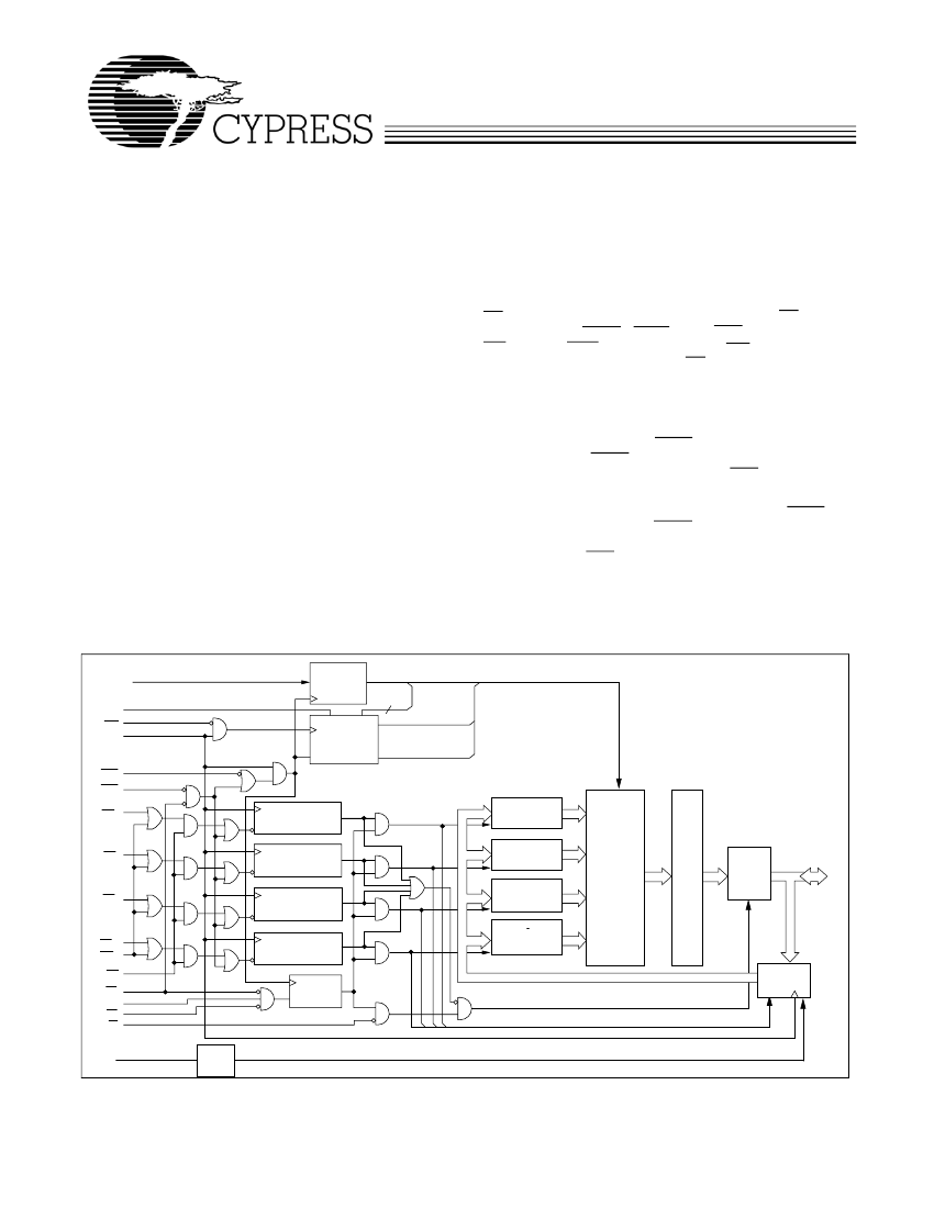
6.5 ns (133-MHz version). A 2-bit on-chip counter captures the
first address in a burst and increments the address automati-
cally for the rest of the burst access. All synchronous inputs
are gated by registers controlled by a positive-edge-triggered
Clock Input (CLK). The synchronous inputs include all
addresses, all data inputs, address-pipelining Chip Enable
(CE
1
), depth-expansion Chip Enables (CE
2
and CE
3
), Burst
Control inputs (ADSC, ADSP, and ADV), Write Enables
(BW
[A:D]
, and BWE), and Global Write (GW). Asynchronous
inputs include the Output Enable (OE) and the ZZ pin.
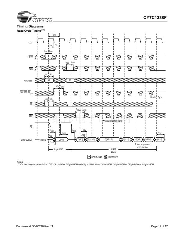
The CY7C1338F allows either interleaved or linear burst
sequences, selected by the MODE input pin. A HIGH selects
an interleaved burst sequence, while a LOW selects a linear
burst sequence. Burst accesses can be initiated with the
Processor Address Strobe (ADSP) or the cache Controller
Address Strobe (ADSC) inputs. Address advancement is
controlled by the Address Advancement (ADV) input.
Addresses and chip enables are registered at rising edge of
clock when either Address Strobe Processor (ADSP) or
Address Strobe Controller (ADSC) are active. Subsequent
burst addresses can be internally generated as controlled by
the Advance pin (ADV).
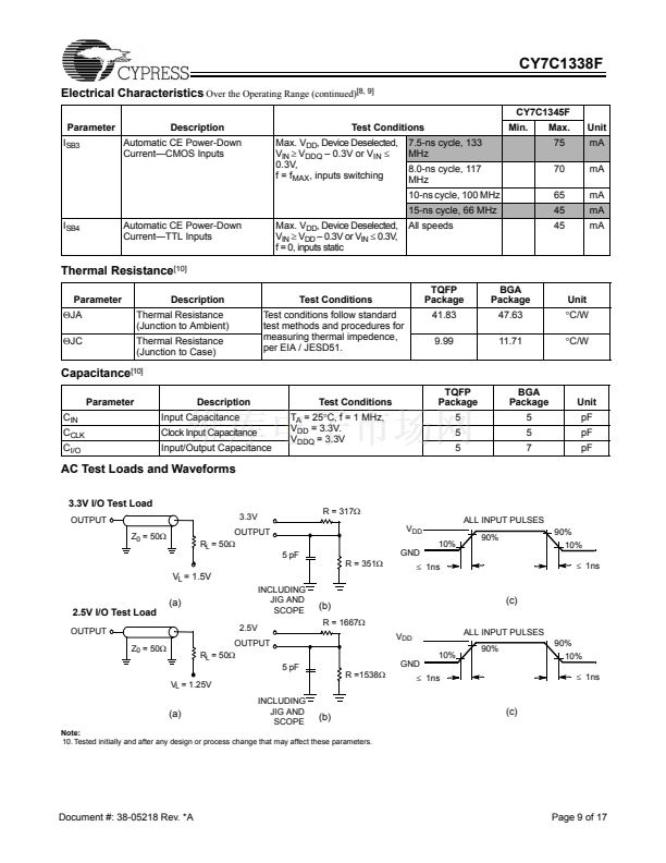
The CY7C1338F operates from a +3.3V core power supply
while all outputs may operate with either a +2.5 or +3.3V
supply. All inputs and outputs are JEDEC-standard
JESD8-5-compatible.
鈥?/div>
鈥?/div>
鈥?/div>
鈥?/div>
鈥?/div>
鈥?/div>
鈥?/div>
Functional Description
[1]
The CY7C1338F is a 131,072 x 32 synchronous cache RAM
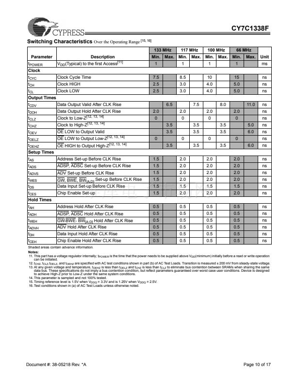
designed to interface with high-speed microprocessors with
minimum glue logic. Maximum access delay from clock rise is
Logic Block Diagram
A0, A1, A
ADDRESS
REGISTER
A
[1:0]
MODE
ADV
CLK
BURST Q1
COUNTER
AND LOGIC
Q0
CLR
ADSC
ADSP
DQ
D
BYTE
BW
D
WRITE REGISTER
DQ
D
BYTE
WRITE REGISTER
BW
C
DQ
C
BYTE
WRITE REGISTER
DQ
C
BYTE
WRITE REGISTER
DQ
B
BYTE
BW
B
DQ
B
BYTE
WRITE REGISTER
DQ
A
BYTE
BW
A
BWE
GW
CE1
CE2
CE3
OE
DQ
A
BYTE
WRITE REGISTER
WRITE REGISTER
WRITE REGISTER
MEMORY
ARRAY
SENSE
AMPS
OUTPUT
BUFFERS
DQs
ENABLE
REGISTER
INPUT
REGISTERS
ZZ
SLEEP
CONTROL
Note:
1. For best鈥損ractices recommendations, please refer to the Cypress application note
System Design Guidelines
on www.cypress.com.
Cypress Semiconductor Corporation
Document #: 38-05218 Rev. *A
鈥?/div>
3901 North First Street
鈥?/div>
San Jose
,
CA 95134
鈥?/div>
408-943-2600
Revised February 2, 2004
CY7C1338相关型号PDF文件下载
-
型号
版本
描述
厂商
下载
-
英文版
16K x 8/9 Dual-Port Static RAM with Sem, Int, Busy
Cypress
-
英文版
32K x 8/9 Dual-Port Static RAM
Cypress
-
英文版
64K/128K x 8/9 Dual-Port Static RAM
CYPRESS
-
英文版
64K/128K x 8/9 Dual-Port Static RAM
CYPRESS [C...
-
英文版
64K/128K x 8/9 Dual-Port Static RAM
CYPRESS
-
英文版
64K/128K x 8/9 Dual-Port Static RAM
CYPRESS [C...
-
英文版
4K x 16/18 and 8K x 16/18 Dual-Port Static RAM with SEM, INT...
CYPRESS
-
英文版
4K x 16/18 and 8K x 16/18 Dual-Port Static RAM with SEM, INT...
CYPRESS [C...
-
英文版
4K x 16/18 and 8K x 16/18 Dual-Port Static RAM with Sem, Int...
Cypress
-
英文版
16K x 16/18 Dual-Port Static RAM
Cypress
-
英文版
32K/64K x 16/18 Dual-Port Static RAM
CYPRESS
-
英文版
32K/64K x 16/18 Dual-Port Static RAM
CYPRESS [C...
-
英文版
32K/64K x 16/18 Dual-Port Static RAM
CYPRESS
-
英文版
32K/64K x 16/18 Dual-Port Static RAM
CYPRESS [C...


 1
1
 2
2
 3
3
 4
4
 5
5
 6
6
 7
7
 8
8
 9
9
 10
10
 11
11
 12
12
 13
13
 14
14
 15
15
 16
16
 17
17
