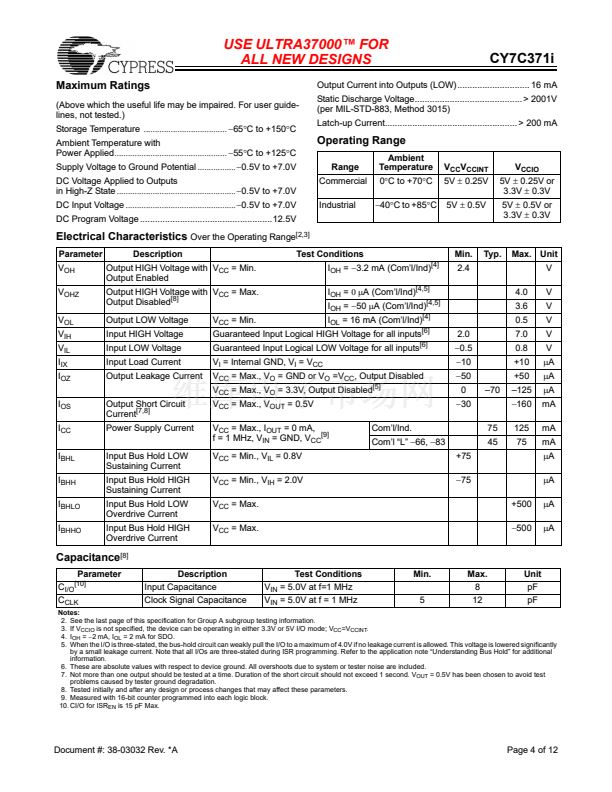
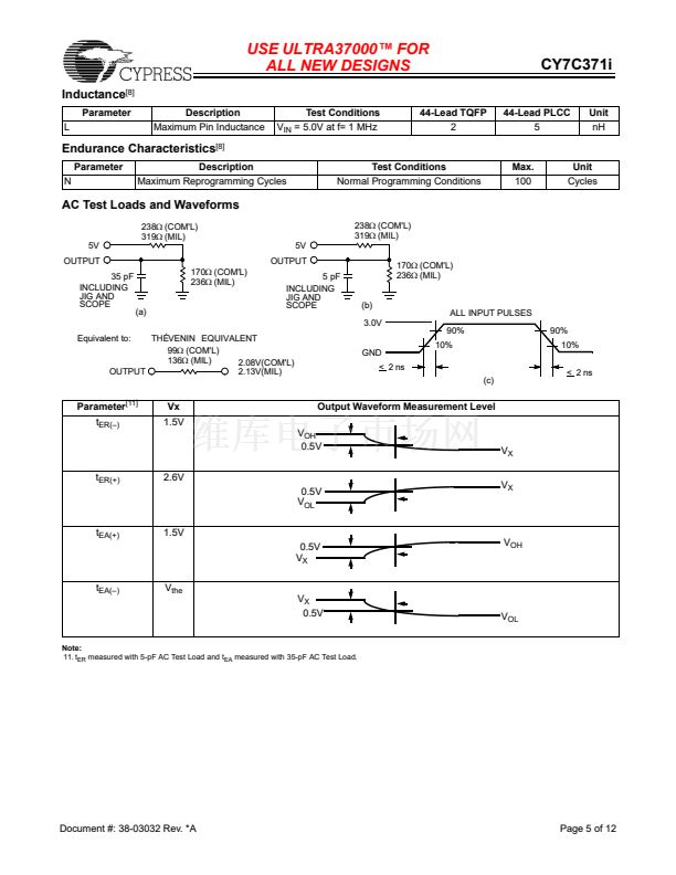
鈥?/div>
t
CO
= 6 ns
Fully PCI-compliant
3.3V or 5.0V I/O operation
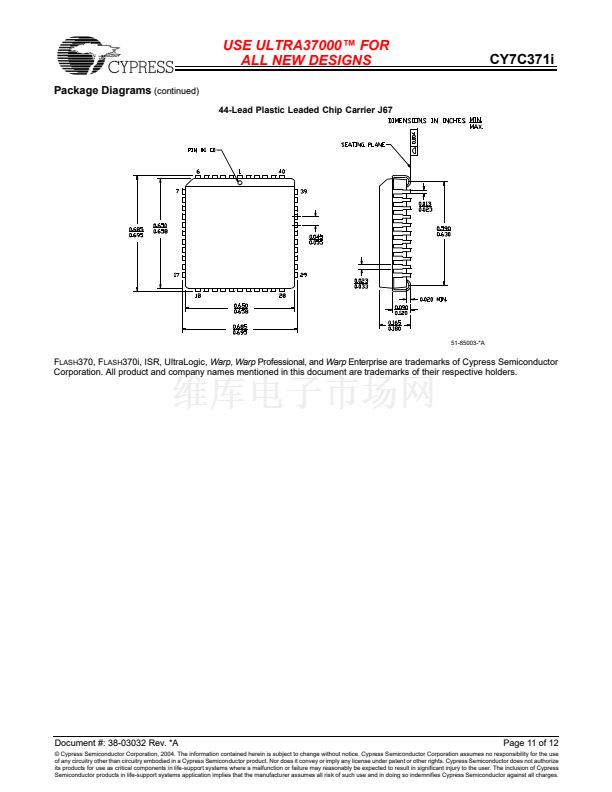
Available in 44-pin PLCC, and TQFP packages
Pin-compatible with the CY7C372i
designed to bring the ease of use and high performance of the
22V10, as well as PCI Local Bus Specification support, to
high-density CPLDs.
Like all of the UltraLogic鈩?F
LASH
370i devices, the CY7C371i
is electrically erasable and In-System Reprogrammable (ISR),
which simplifies both design and manufacturing flows, thereby
reducing costs. The Cypress ISR function is implemented
through a JTAG serial interface. Data is shifted in and out
through the SDI and SDO pins. The ISR interface is enabled
using the programming voltage pin (ISR
EN
). Additionally,
because of the superior routability of the F
LASH
370i devices,
ISR often allows users to change existing logic designs while
simultaneously fixing pinout assignments.
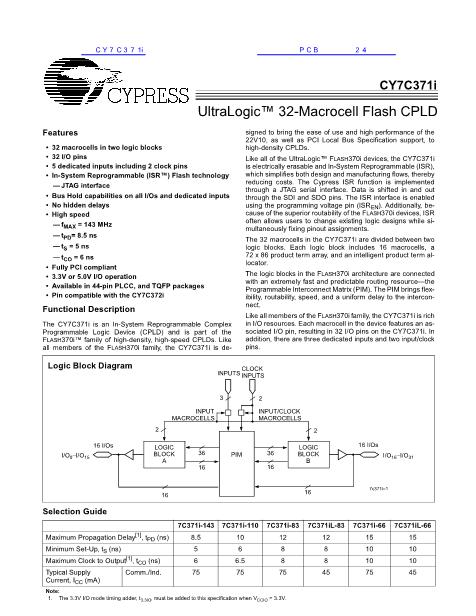
The 32 macrocells in the CY7C371i are divided between two
logic blocks. Each logic block includes 16 macrocells, a
72 x 86 product term array, and an intelligent product term
allocator.
The logic blocks in the F
LASH
370i architecture are connected
with an extremely fast and predictable routing resource鈥攖he
Programmable Interconnect Matrix (PIM). The PIM brings
flexibility, routability, speed, and a uniform delay to the inter-
connect.
Like all members of the F
LASH
370i family, the CY7C371i is rich
in I/O resources. Each macrocell in the device features an
associated I/O pin, resulting in 32 I/O pins on the CY7C371i.
In addition, there are three dedicated inputs and two
input/clock pins.
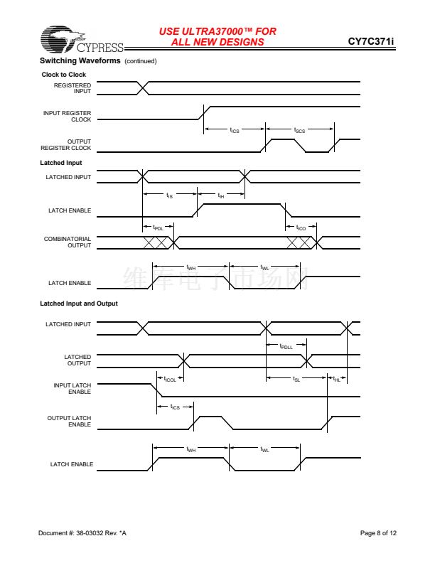
Clock
Inputs
鈥?/div>
鈥?/div>
鈥?/div>
鈥?/div>
Functional Description
The CY7C371i is an In-System Reprogrammable Complex
Programmable Logic Device (CPLD) and is part of the
F
LASH
370i鈩?family of high-density, high-speed CPLDs. Like
all members of the F
LASH
370i family, the CY7C371i is
Logic Block Diagram
Inputs
3
INPUT
MACROCELLS
2
16 I/Os
I/O
0
鈥揑/O
15
LOGIC
BLOCK
A
2
INPUT/CLOCK
MACROCELLS
2
LOGIC
BLOCK
B
16 I/Os
I/O
16
鈥揑/O
31
36
16
PIM
36
16
16
16
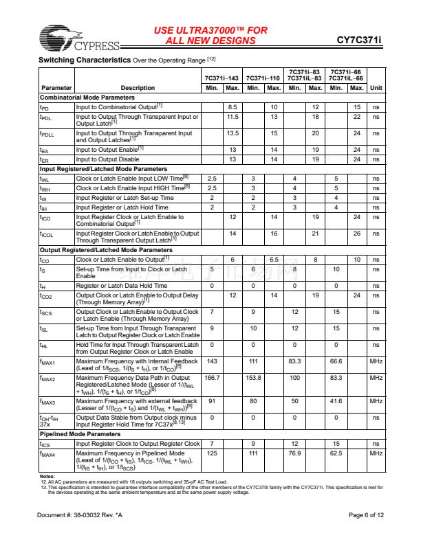
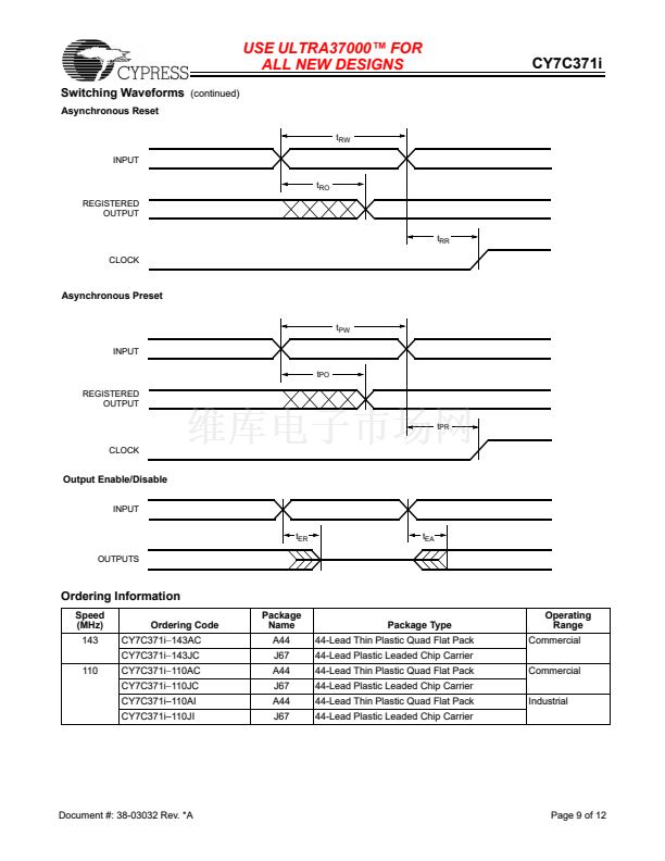
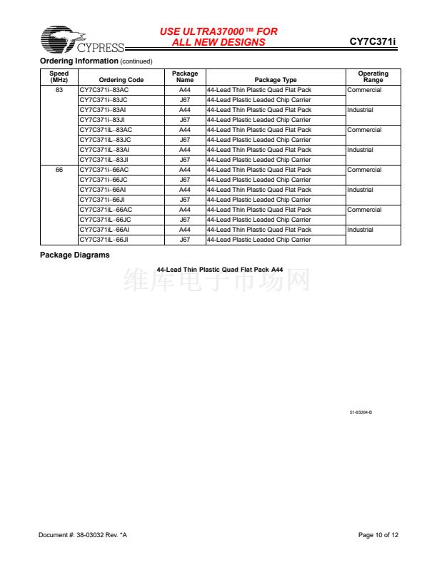
Selection Guide
7C371i-143 7C371i-110 7C371i-83 7C371iL-83 7C371i-66 7C371iL-66
Maximum Propagation Delay
[1]
, t
PD
Minimum Set-up, t
S
Maximum Clock to
Output
[1]
,
t
CO
Typical Supply Current, I
CC
Comm./Ind.
8.5
5
6
75
10
6
6.5
75
12
8
8
75
12
8
8
45
15
10
10
75
15
10
10
45
Unit
ns
ns
ns
mA
Note:
1. The 3.3V I/O mode timing adder, t
3.3IO
, must be added to this specification when V
CCIO
= 3.3V.
Cypress Semiconductor Corporation
Document #: 38-03032 Rev. *A
鈥?/div>
3901 North First Street
鈥?/div>
San Jose
,
CA 95134
鈥?/div>
408-943-2600
Revised April 19, 2004
CY7C371i相关型号PDF文件下载
-
型号
版本
描述
厂商
下载
-
英文版
16K x 8/9 Dual-Port Static RAM with Sem, Int, Busy
Cypress
-
英文版
32K x 8/9 Dual-Port Static RAM
Cypress
-
英文版
64K/128K x 8/9 Dual-Port Static RAM
CYPRESS
-
英文版
64K/128K x 8/9 Dual-Port Static RAM
CYPRESS [C...
-
英文版
64K/128K x 8/9 Dual-Port Static RAM
CYPRESS
-
英文版
64K/128K x 8/9 Dual-Port Static RAM
CYPRESS [C...
-
英文版
4K x 16/18 and 8K x 16/18 Dual-Port Static RAM with SEM, INT...
CYPRESS
-
英文版
4K x 16/18 and 8K x 16/18 Dual-Port Static RAM with SEM, INT...
CYPRESS [C...
-
英文版
4K x 16/18 and 8K x 16/18 Dual-Port Static RAM with Sem, Int...
Cypress
-
英文版
16K x 16/18 Dual-Port Static RAM
Cypress
-
英文版
32K/64K x 16/18 Dual-Port Static RAM
CYPRESS
-
英文版
32K/64K x 16/18 Dual-Port Static RAM
CYPRESS [C...
-
英文版
32K/64K x 16/18 Dual-Port Static RAM
CYPRESS
-
英文版
32K/64K x 16/18 Dual-Port Static RAM
CYPRESS [C...


 1
1
 2
2
 3
3
 4
4
 5
5
 6
6
 7
7
 8
8
 9
9
 10
10
 11
11
 12
12
