words. Both the CY7C403 and CY7C404 have an output en-
able (OE) function.
鈥?/div>
DI
n
) under the control of the shift in (SI) input. The stored
words stack up at the output (DO
0
鈥?DO
n
) in the order they
were entered. A read command on the shift out (SO) input
causes the next to last word to move to the output and all data
shifts down once in the stack. The input ready (IR) signal acts
as a flag to indicate when the input is ready to accept new data
(HIGH), to indicate when the FIFO is full (LOW), and to provide
a signal for a cascading. The output ready (OR) signal is a flag
to indicate the output contains valid data (HIGH), to indicate
the FIFO is empty (LOW), and to provide a signal for cascad-
ing.
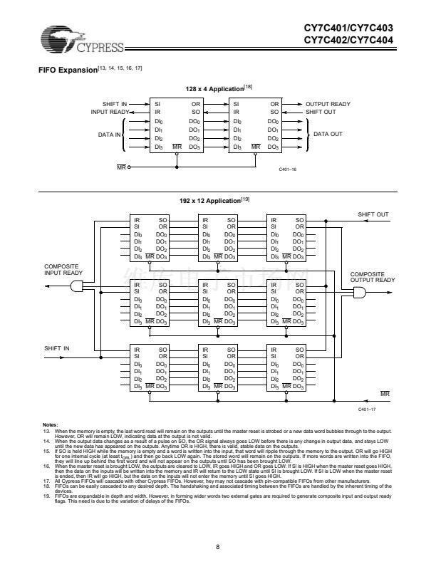
Parallel expansion for wider words is accomplished by logical-
ly ANDing the IR and OR signals to form composite signals.
Serial expansion is accomplished by tying the data inputs of
one device to the data outputs of the previous device. The IR
pin of the receiving device is connected to the SO pin of the
sending device, and the OR pin of the sending device is con-
nected to the SI pin of the receiving device.
Reading and writing operations are completely asynchronous,
allowing the FIFO to be used as a buffer between two digital
machines of widely differing operating frequencies. The
25-MHz operation makes these FIFOs ideal for high-speed
communication and controller applications.
Functional Description
The CY7C401 and CY7C403 are asynchronous first-in
first-out (FIFOs) organized as 64 four-bit words. The CY7C402
and CY7C404 are similar FIFOs organized as 64 five-bit
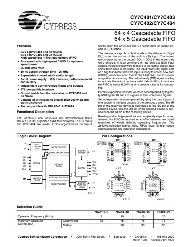
Logic Block Diagram
SI
IR
INPUT
CONTROL
LOGIC
Pin Configurations
DIP
WRITE POINTER
(CY7C401) NC
(CY7C403) OE
IR
SI
DI
0
DI
1
DI
2
DI
3
GND
1
16
2
15
3
14
4 CY7C401
13
CY7C403
5
12
6
11
10
7
9
8
VCC
SO
OR
DO
0
DO
1
DO
2
DO
3
MR
(CY7C402) NC
(CY7C404) OE
IR
SI
DI
0
DI
1
DI
2
DI
3
DI
4
GND
DIP
1
18
2
17
3
16
4 CY7C402
15
CY7C404
5
14
6
13
12
7
11
8
10
9
VCC
SO
OR
DO
0
DO
1
DO
2
DO
3
DO
4
MR
WRITE MULTIPLEXER
DI 0
DI 1
DI 2
DI 3
(DI 4)
DATAIN
MEMORY
ARRAY
OUTPUT
ENABLE
OE
DO0
DO1
DATA
IN
DO2
DO3
(DO 4)
C401鈥?
C401鈥?
LCC
LCC
MR
MASTER
RESET
READ MULTIPLEXER
OUTPUT
CONTROL
LOGIC
SO
OR
C401鈥?
SI
DI
0
DI
1
DI
2
NC
READ POINTER
3 2 1 2019
4
18 NC
5
17 OR
CY7C401
6 CY7C403 16 DO
0
7
15 DO
1
8
14 DO
2
910111213
SI
DI
0
DI
1
DI
2
DI
3
3 2 1 2019
4
18 OR
5
17 DO
0
6 CY7C402 16 DO
1
7 CY7C404 15 DO
2
8
14 DO
3
910111213
C401鈥?
C401鈥?
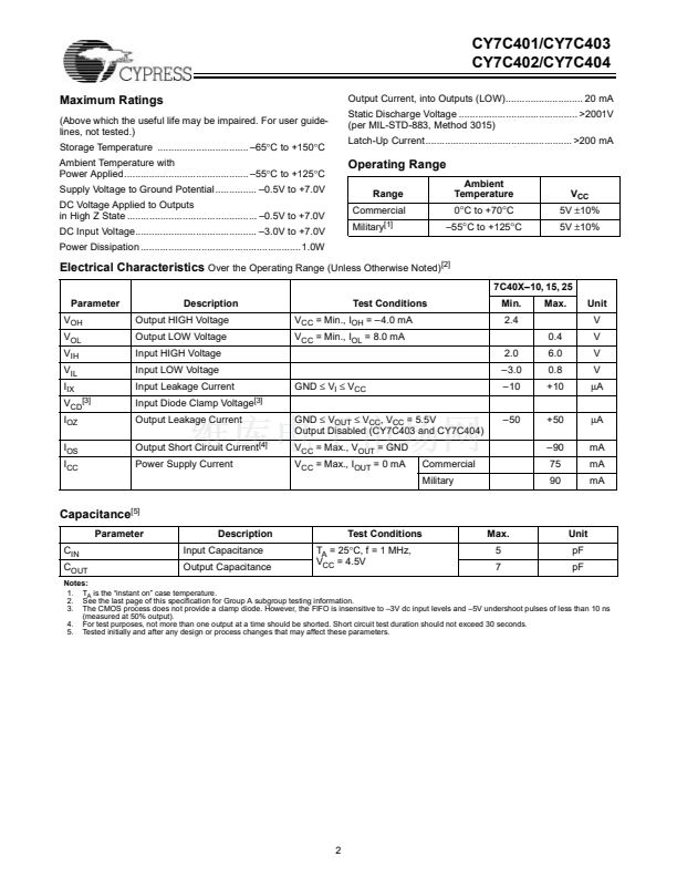
Selection Guide
7C401/2鈥?
Operating Frequency (MHz)
Maximum Operating
Current (mA)
Commercial
Military
5
75
7C40X鈥?0
10
75
90
7C40X鈥?5
15
75
90
7C40X鈥?5
25
75
90
Cypress Semiconductor Corporation
鈥?/div>
3901 North First Street
鈥?/div>
San Jose
鈥?/div>
CA 95134 鈥?/div>
408-943-2600
March 1986 鈥?Revised April 1995


 1
1
 2
2
 3
3
 4
4
 5
5
 6
6
 7
7
 8
8
 9
9
 10
10
 11
11
 12
12
 13
13
